Documentation
Everything you need to build your first circuit and keep experimenting.
Sign in with Google to enter the playground. Free accounts get 25 simulation starts per seven-day window; Pro includes unlimited starts, saving and protected lab imports. Check your profile, allowance, expiry and payments in Settings.
Getting started
- Open the playground and drag a battery, resistor and LED from the library.
- Connect battery + to a resistor, resistor to LED anode (A), and LED cathode (K) to battery −.
- Use a series resistor, such as 330 Ω with the default 5 V battery.
- Choose Start simulation. Select the LED to see its current and voltage.
Or open a ready-made example and change one thing at a time.
Breadboard connections
The default full-size board has 830 contacts and 63 columns (630 strip contacts and 200 rail contacts). Within each column, a–e are connected, and f–j form a separate connection. The centre gap separates the sides. Adjacent columns are isolated.
The four power rails are independent. Their + and − labels do not supply electricity: connect a source. Split power rails divides each rail in half; a jumper can reconnect them. DIP ICs sit across the centre gap.
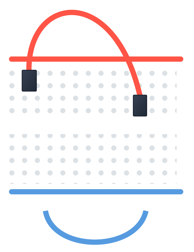
Wire crossings do not connect electrically. Only endpoint terminals make connections.
Workspace controls
| Action | Control |
|---|---|
| Place / move | Click a library card, then click the workspace to place it, or drag it directly. Connected wire endpoints follow moving components. |
| Connect | Click a hole or pin, then another terminal. The finished wire is selected for editing. |
| Shape a wire | Click empty space, inside or outside the breadboard, while drawing to add bends. Auto-Set routes around component bodies and prefers separate lanes. Crossings have a white break; they are not junctions. |
| Schematic | Switch to Schematic for gate symbols and pin blocks. Matching net labels are connected; select a label to highlight its terminals. The diagram includes breadboard strips and power rails. |
| Wire colour | Finish or select a wire, then choose a preset or custom colour in Properties. |
| Reconnect | Drag either circular wire endpoint. Invalid drops keep the original connection. |
| Return to Select | Click empty background when no wire is in progress. Select or Escape also cancels an unfinished wire. |
| Select a group | Drag a rectangle from blank space; Shift adds to the selection. |
| Pan / zoom | Two-finger scrolling pans. Pinch or Ctrl/Command + scroll zooms. Space + drag also pans. |
| Undo / redo | Ctrl/Command + Z; Ctrl/Command + Shift + Z. |
| Rename | Click the circuit title. Enter or clicking away saves; Escape cancels. |
Components & instruments
The SVG library contains 113 components across sensors, outputs, power, breadboards, controllers, instruments and ICs. Search a familiar name or a part number: 7432, 74HC32 and OR gate IC find the same component. Common aliases include LDR, DSO and multimeter. TTL/LS numbers are search aliases for the displayed HC device; electrical specifications remain those of the displayed model.
Sensor values, DIP contacts and keypad keys are adjustable in Properties. Added breadboards have 830, 400 or 170 contacts, with isolated strips and rails. Gate, latch, counter, shift-register, adder and timer models use the labeled pins. Transistors, motors and analog ICs use simplified educational models.
Browse descriptions and pin functions for every component ↓
Wiring only: Arduino, micro:bit and ATtiny can be placed and connected, but do not execute firmware. LCDs, NeoPixels, the IR remote, clock display and I²C expander do not yet decode their control protocols. Their cards and Properties identify this limitation.
Resistors, LEDs, capacitors, diodes, potentiometers, batteries, switches, pushbuttons and seven-segment displays are available. Select a component to change its settings. Double-click a switch to toggle it.
Logic lab
74HC08/32/86/00/04/02/10 model powered gates. Connect pin 14 to 2–6 V and pin 7 to ground; tie unused inputs HIGH or LOW. Hover over terminals to see their functions.
CD4511 uses pin 16 for its 3–18 V supply and pin 8 for ground. Its BCD inputs drive a common-cathode display through one resistor per segment. Lamp test, blanking and latch controls work. Display Properties also supports common-anode circuits.
Measure your circuit
The function generator produces sine, square and triangle signals with adjustable amplitude, frequency and offset. Connect OUT and GND. The scope reads CH1 and CH2 relative to GND. Its graph opens when a scope is placed; drag its header or minimise it. Export samples downloads CSV. The voltmeter reads voltage between + and −.
Component & pin reference
113 of 113 components
Open a component to read its description and pin functions. IC pin numbers match the playground’s DIP package; count counterclockwise from pin 1 when viewed from above. Board and module rows use their printed terminal labels. Breadboard rows and rails are grouped to explain every contact without repeating hundreds of identical entries.
General
ResistorEducational model
A resistor limits current and produces a voltage drop. Use it for LED current limiting, voltage dividers and pull-up or pull-down inputs.
Connecting it: Use the terminal labels in the playground and select the part to adjust its available Properties. Wire crossings alone do not create connections.
| Pin / terminal | Function & connection |
|---|---|
| 1 | One end of the two-terminal element. Connect the other end into your circuit; this element is non-polarized. |
| 2 | One end of the two-terminal element. Connect the other end into your circuit; this element is non-polarized. |
These tables describe the playground footprint. Some modules use a simplified connector layout; check the specific manufacturer’s pinout when moving a circuit to physical hardware.
CapacitorEducational model
A non-polarized capacitor stores charge between two terminals. Use it for filters, timing and smoothing; its voltage changes over time when charged through a resistor.
Connecting it: Use the terminal labels in the playground and select the part to adjust its available Properties. Wire crossings alone do not create connections.
| Pin / terminal | Function & connection |
|---|---|
| 1 | One end of the two-terminal element. Connect the other end into your circuit; this element is non-polarized. |
| 2 | One end of the two-terminal element. Connect the other end into your circuit; this element is non-polarized. |
These tables describe the playground footprint. Some modules use a simplified connector layout; check the specific manufacturer’s pinout when moving a circuit to physical hardware.
Silicon diodeEducational model
A silicon diode conducts primarily from anode to cathode. Use it for rectification, current steering and protection; the playground uses an adjustable forward-voltage threshold.
Connecting it: Use the terminal labels in the playground and select the part to adjust its available Properties. Wire crossings alone do not create connections.
| Pin / terminal | Function & connection |
|---|---|
| A | Anode (+). Forward current enters here and leaves through K; use current limiting for an LED. |
| K | Cathode (−). The diode’s band marks this terminal. |
These tables describe the playground footprint. Some modules use a simplified connector layout; check the specific manufacturer’s pinout when moving a circuit to physical hardware.
Polarized capacitorEducational model
An electrolytic capacitor stores charge with a required polarity. Use it for supply smoothing and longer timing intervals. Connect + toward the higher potential and − toward the lower potential.
Connecting it: Use the terminal labels in the playground and select the part to adjust its available Properties. Wire crossings alone do not create connections.
| Pin / terminal | Function & connection |
|---|---|
| + | Positive terminal; connect to the positive side of the intended circuit. |
| − | Negative / return terminal; connect to the return side of the intended circuit. |
These tables describe the playground footprint. Some modules use a simplified connector layout; check the specific manufacturer’s pinout when moving a circuit to physical hardware.
Zener diodeEducational model
Forward diode and reverse breakdown model. Cathode K is the banded end.
Connecting it: Use the terminal labels in the playground and select the part to adjust its available Properties. Wire crossings alone do not create connections.
| Pin / terminal | Function & connection |
|---|---|
| A | Anode (+). Forward current enters here and leaves through K; use current limiting for an LED. |
| K | Cathode (−). The diode’s band marks this terminal. |
These tables describe the playground footprint. Some modules use a simplified connector layout; check the specific manufacturer’s pinout when moving a circuit to physical hardware.
InductorEducational model
Stores magnetic energy. Transient model includes 1 Ω winding resistance.
Connecting it: Use the terminal labels in the playground and select the part to adjust its available Properties. Wire crossings alone do not create connections.
| Pin / terminal | Function & connection |
|---|---|
| 1 | One end of the two-terminal element. Connect the other end into your circuit; this element is non-polarized. |
| 2 | One end of the two-terminal element. Connect the other end into your circuit; this element is non-polarized. |
These tables describe the playground footprint. Some modules use a simplified connector layout; check the specific manufacturer’s pinout when moving a circuit to physical hardware.
Input
PotentiometerEducational model
An adjustable resistor with a sliding middle contact. Use the wiper as a variable voltage-divider output or use it with one end as a variable resistance.
Connecting it: Use the terminal labels in the playground and select the part to adjust its available Properties. Wire crossings alone do not create connections.
| Pin / terminal | Function & connection |
|---|---|
| A | Fixed end A of the resistance track. Connect A and B across a supply for a divider. |
| W | Wiper: adjustable contact between A and B. Use it as the voltage-divider output. |
| B | Fixed end B of the resistance track. Connect A and B across a supply for a divider. |
These tables describe the playground footprint. Some modules use a simplified connector layout; check the specific manufacturer’s pinout when moving a circuit to physical hardware.
Slide switchEducational model
SPST switch. Toggle in the inspector, or double-click its body.
Connecting it: Use the terminal labels in the playground and select the part to adjust its available Properties. Wire crossings alone do not create connections.
| Pin / terminal | Function & connection |
|---|---|
| 1 | Switch contact. It connects to the other contact when closed and is isolated when open. |
| 2 | Switch contact. It connects to the other contact when closed and is isolated when open. |
These tables describe the playground footprint. Some modules use a simplified connector layout; check the specific manufacturer’s pinout when moving a circuit to physical hardware.
Photoresistor · LDREducational model
Light-dependent resistor. Set its resistance to represent illumination; non-polarized.
Connecting it: Set the environment or resistance in Properties. Read an analog output with a meter or scope; passive resistive sensors normally need a voltage divider.
| Pin / terminal | Function & connection |
|---|---|
| 1 | One end of the two-terminal element. Connect the other end into your circuit; this element is non-polarized. |
| 2 | One end of the two-terminal element. Connect the other end into your circuit; this element is non-polarized. |
These tables describe the playground footprint. Some modules use a simplified connector layout; check the specific manufacturer’s pinout when moving a circuit to physical hardware.
PhotodiodeEducational model
Reverse-biased light sensor. Adjustable photocurrent flows from cathode to anode.
Connecting it: Use the terminal labels in the playground and select the part to adjust its available Properties. Wire crossings alone do not create connections.
| Pin / terminal | Function & connection |
|---|---|
| A | Anode (+). Forward current enters here and leaves through K; use current limiting for an LED. |
| K | Cathode (−). The diode’s band marks this terminal. |
These tables describe the playground footprint. Some modules use a simplified connector layout; check the specific manufacturer’s pinout when moving a circuit to physical hardware.
Ambient light sensorEducational model
A powered light-sensing module. Its output represents the light level selected in Properties.
Connecting it: Set the environment or resistance in Properties. Read an analog output with a meter or scope; passive resistive sensors normally need a voltage divider.
| Pin / terminal | Function & connection |
|---|---|
| VCC | Positive supply input. Connect to the appropriate source for this component. |
| OUT | Sensor signal output, set by the environment control in Properties. |
| GND | Ground / supply return; use the circuit’s reference node. |
These tables describe the playground footprint. Some modules use a simplified connector layout; check the specific manufacturer’s pinout when moving a circuit to physical hardware.
Flex sensorEducational model
Variable resistance models bending. Read with a voltage divider.
Connecting it: Set the environment or resistance in Properties. Read an analog output with a meter or scope; passive resistive sensors normally need a voltage divider.
| Pin / terminal | Function & connection |
|---|---|
| 1 | One end of the two-terminal element. Connect the other end into your circuit; this element is non-polarized. |
| 2 | One end of the two-terminal element. Connect the other end into your circuit; this element is non-polarized. |
These tables describe the playground footprint. Some modules use a simplified connector layout; check the specific manufacturer’s pinout when moving a circuit to physical hardware.
Force sensor · FSREducational model
Force-sensitive resistance. Reduce resistance to represent greater pressure.
Connecting it: Set the environment or resistance in Properties. Read an analog output with a meter or scope; passive resistive sensors normally need a voltage divider.
| Pin / terminal | Function & connection |
|---|---|
| 1 | One end of the two-terminal element. Connect the other end into your circuit; this element is non-polarized. |
| 2 | One end of the two-terminal element. Connect the other end into your circuit; this element is non-polarized. |
These tables describe the playground footprint. Some modules use a simplified connector layout; check the specific manufacturer’s pinout when moving a circuit to physical hardware.
IR sensorEducational model
A powered infrared detection module. Adjust Detection in Properties to represent an object or infrared source being detected.
Connecting it: Set the environment or resistance in Properties. Read an analog output with a meter or scope; passive resistive sensors normally need a voltage divider.
| Pin / terminal | Function & connection |
|---|---|
| VCC | Positive supply input. Connect to the appropriate source for this component. |
| OUT | Sensor signal output, set by the environment control in Properties. |
| GND | Ground / supply return; use the circuit’s reference node. |
These tables describe the playground footprint. Some modules use a simplified connector layout; check the specific manufacturer’s pinout when moving a circuit to physical hardware.
Ultrasonic distance sensor · HC-SR04Educational model
An HC-SR04 style distance module sends an ultrasonic burst after a trigger and returns an echo pulse representing the distance setting.
Connecting it: Set the environment or resistance in Properties. Read an analog output with a meter or scope; passive resistive sensors normally need a voltage divider.
| Pin / terminal | Function & connection |
|---|---|
| VCC | Positive supply input. Connect to the appropriate source for this component. |
| TRIG | Distance measurement trigger input; drives the modeled trigger when HIGH. |
| ECHO | Distance-dependent echo pulse output after a trigger. |
| GND | Ground / supply return; use the circuit’s reference node. |
These tables describe the playground footprint. Some modules use a simplified connector layout; check the specific manufacturer’s pinout when moving a circuit to physical hardware.
Ultrasonic distance sensor · 3-pinEducational model
A three-terminal distance module combines trigger and echo on one signal line. The playground uses the Properties trigger control to initiate a modeled distance pulse.
Connecting it: Set the environment or resistance in Properties. Read an analog output with a meter or scope; passive resistive sensors normally need a voltage divider.
| Pin / terminal | Function & connection |
|---|---|
| GND | Ground / supply return; use the circuit’s reference node. |
| 5V | Positive 5 V supply contact. |
| SIG | Shared trigger/echo connection. Use Trigger in Properties for the simplified model. |
These tables describe the playground footprint. Some modules use a simplified connector layout; check the specific manufacturer’s pinout when moving a circuit to physical hardware.
PIR motion sensorEducational model
A passive-infrared motion module. Adjust Motion in Properties; its signal indicates the modeled detection state.
Connecting it: Set the environment or resistance in Properties. Read an analog output with a meter or scope; passive resistive sensors normally need a voltage divider.
| Pin / terminal | Function & connection |
|---|---|
| SIG | Sensor signal output; detection is adjusted in Properties. |
| VCC | Positive supply input. Connect to the appropriate source for this component. |
| GND | Ground / supply return; use the circuit’s reference node. |
These tables describe the playground footprint. Some modules use a simplified connector layout; check the specific manufacturer’s pinout when moving a circuit to physical hardware.
Soil moisture sensorEducational model
A powered soil-moisture module. The Moisture setting controls its modeled output level.
Connecting it: Set the environment or resistance in Properties. Read an analog output with a meter or scope; passive resistive sensors normally need a voltage divider.
| Pin / terminal | Function & connection |
|---|---|
| VCC | Positive supply input. Connect to the appropriate source for this component. |
| OUT | Sensor signal output, set by the environment control in Properties. |
| GND | Ground / supply return; use the circuit’s reference node. |
These tables describe the playground footprint. Some modules use a simplified connector layout; check the specific manufacturer’s pinout when moving a circuit to physical hardware.
Tilt sensor · SW-200DEducational model
Tilt-operated contact. Toggle tilted/contact state in Properties.
Connecting it: Use the terminal labels in the playground and select the part to adjust its available Properties. Wire crossings alone do not create connections.
| Pin / terminal | Function & connection |
|---|---|
| 1 | Tilt-operated contact. The Properties state opens or closes the pair. |
| 2 | Tilt-operated contact. The Properties state opens or closes the pair. |
These tables describe the playground footprint. Some modules use a simplified connector layout; check the specific manufacturer’s pinout when moving a circuit to physical hardware.
Temperature sensor · TMP36Educational model
TMP36 educational model: OUT = 0.5 V + 10 mV/°C. Connect VCC, OUT and GND; set temperature in Properties.
Connecting it: Set the environment or resistance in Properties. Read an analog output with a meter or scope; passive resistive sensors normally need a voltage divider.
| Pin / terminal | Function & connection |
|---|---|
| VCC | Positive supply input. Connect to the appropriate source for this component. |
| OUT | Sensor signal output, set by the environment control in Properties. |
| GND | Ground / supply return; use the circuit’s reference node. |
These tables describe the playground footprint. Some modules use a simplified connector layout; check the specific manufacturer’s pinout when moving a circuit to physical hardware.
Gas sensor · MQ-2Educational model
An MQ-2 style sensor combines a heater with a gas-sensitive resistance. The Gas level setting changes the sensing resistance; the two copies of each electrode share their side of the sensing element.
Connecting it: Set the environment or resistance in Properties. Read an analog output with a meter or scope; passive resistive sensors normally need a voltage divider.
| Pin / terminal | Function & connection |
|---|---|
| A1 | Sensing electrode A. Both A terminals represent the same side of the sensing resistor. Use A and B in a voltage divider. |
| H1 | Heater terminal. Apply heater power across H1 and H2; the model includes a heater load. |
| A2 | Sensing electrode A. Both A terminals represent the same side of the sensing resistor. Use A and B in a voltage divider. |
| B1 | Sensing electrode B. Both B terminals represent the same side of the sensing resistor. Use A and B in a voltage divider. |
| H2 | Heater terminal. Apply heater power across H1 and H2; the model includes a heater load. |
| B2 | Sensing electrode B. Both B terminals represent the same side of the sensing resistor. Use A and B in a voltage divider. |
These tables describe the playground footprint. Some modules use a simplified connector layout; check the specific manufacturer’s pinout when moving a circuit to physical hardware.
Keypad 4 × 4Educational model
A selected key closes one row/column contact. Choose the key in Properties.
Connecting it: Use the terminal labels in the playground and select the part to adjust its available Properties. Wire crossings alone do not create connections.
| Pin / terminal | Function & connection |
|---|---|
| R1 | Matrix row 1. Selecting a key connects this row to that key’s column; rows are not automatically joined. |
| R2 | Matrix row 2. Selecting a key connects this row to that key’s column; rows are not automatically joined. |
| R3 | Matrix row 3. Selecting a key connects this row to that key’s column; rows are not automatically joined. |
| R4 | Matrix row 4. Selecting a key connects this row to that key’s column; rows are not automatically joined. |
| C1 | Matrix column 1. Selecting a key connects this column to that key’s row; scan rows/columns in a physical circuit. |
| C2 | Matrix column 2. Selecting a key connects this column to that key’s row; scan rows/columns in a physical circuit. |
| C3 | Matrix column 3. Selecting a key connects this column to that key’s row; scan rows/columns in a physical circuit. |
| C4 | Matrix column 4. Selecting a key connects this column to that key’s row; scan rows/columns in a physical circuit. |
These tables describe the playground footprint. Some modules use a simplified connector layout; check the specific manufacturer’s pinout when moving a circuit to physical hardware.
DIP switch · DPSTEducational model
Two independent contacts. Choose which contacts are closed in Properties.
Connecting it: Use the terminal labels in the playground and select the part to adjust its available Properties. Wire crossings alone do not create connections.
| Pin / terminal | Function & connection |
|---|---|
| 1 1A | Contact 1 1A: pairs with 1B. Its Properties switch closes only this contact pair. |
| 2 2A | Contact 2 2A: pairs with 2B. Its Properties switch closes only this contact pair. |
| 3 2B | Contact 3 2B: pairs with 3A. Its Properties switch closes only this contact pair. |
| 4 1B | Contact 4 1B: pairs with 4A. Its Properties switch closes only this contact pair. |
These tables describe the playground footprint. Some modules use a simplified connector layout; check the specific manufacturer’s pinout when moving a circuit to physical hardware.
DIP switch · SPST × 4Educational model
Four independently controlled contacts.
Connecting it: Use the terminal labels in the playground and select the part to adjust its available Properties. Wire crossings alone do not create connections.
| Pin / terminal | Function & connection |
|---|---|
| 1 1A | Contact 1 1A: pairs with 1B. Its Properties switch closes only this contact pair. |
| 2 2A | Contact 2 2A: pairs with 2B. Its Properties switch closes only this contact pair. |
| 3 3A | Contact 3 3A: pairs with 3B. Its Properties switch closes only this contact pair. |
| 4 4A | Contact 4 4A: pairs with 4B. Its Properties switch closes only this contact pair. |
| 5 4B | Contact 5 4B: pairs with 5A. Its Properties switch closes only this contact pair. |
| 6 3B | Contact 6 3B: pairs with 6A. Its Properties switch closes only this contact pair. |
| 7 2B | Contact 7 2B: pairs with 7A. Its Properties switch closes only this contact pair. |
| 8 1B | Contact 8 1B: pairs with 8A. Its Properties switch closes only this contact pair. |
These tables describe the playground footprint. Some modules use a simplified connector layout; check the specific manufacturer’s pinout when moving a circuit to physical hardware.
DIP switch · SPST × 6Educational model
Six independently controlled contacts.
Connecting it: Use the terminal labels in the playground and select the part to adjust its available Properties. Wire crossings alone do not create connections.
| Pin / terminal | Function & connection |
|---|---|
| 1 1A | Contact 1 1A: pairs with 1B. Its Properties switch closes only this contact pair. |
| 2 2A | Contact 2 2A: pairs with 2B. Its Properties switch closes only this contact pair. |
| 3 3A | Contact 3 3A: pairs with 3B. Its Properties switch closes only this contact pair. |
| 4 4A | Contact 4 4A: pairs with 4B. Its Properties switch closes only this contact pair. |
| 5 5A | Contact 5 5A: pairs with 5B. Its Properties switch closes only this contact pair. |
| 6 6A | Contact 6 6A: pairs with 6B. Its Properties switch closes only this contact pair. |
| 7 6B | Contact 7 6B: pairs with 7A. Its Properties switch closes only this contact pair. |
| 8 5B | Contact 8 5B: pairs with 8A. Its Properties switch closes only this contact pair. |
| 9 4B | Contact 9 4B: pairs with 9A. Its Properties switch closes only this contact pair. |
| 10 3B | Contact 10 3B: pairs with 1A. Its Properties switch closes only this contact pair. |
| 11 2B | Contact 11 2B: pairs with 1A. Its Properties switch closes only this contact pair. |
| 12 1B | Contact 12 1B: pairs with 1A. Its Properties switch closes only this contact pair. |
These tables describe the playground footprint. Some modules use a simplified connector layout; check the specific manufacturer’s pinout when moving a circuit to physical hardware.
IR remoteWiring only
A handheld infrared remote sends encoded commands to an IR receiver in a physical circuit. This playground provides its visual footprint; it has no external electrical terminals or simulated infrared commands.
Connecting it: The table explains the physical interface, but this part is wiring only in the playground. Serial commands, display updates and data forwarding are not simulated.
This component has no external electrical pins in the playground.
These tables describe the playground footprint. Some modules use a simplified connector layout; check the specific manufacturer’s pinout when moving a circuit to physical hardware.
Output
LEDEducational model
A light-emitting diode glows when forward current flows from anode to cathode. Choose its color in Properties and use a series resistor to limit current.
Connecting it: Put a separate current-limiting resistor in each LED path. Check polarity; the seven-segment common mode is selectable in Properties.
| Pin / terminal | Function & connection |
|---|---|
| A | Anode (+). Forward current enters here and leaves through K; use current limiting for an LED. |
| K | Cathode (−). The diode’s band marks this terminal. |
These tables describe the playground footprint. Some modules use a simplified connector layout; check the specific manufacturer’s pinout when moving a circuit to physical hardware.
7-segment displayEducational model
Eight LED segments including decimal point. Common cathode by default; change to common anode in Properties. Use one series resistor per segment. Pins: 1=e, 2=d, 3=COM, 4=c, 5=DP, 6=b, 7=a, 8=COM, 9=f, 10=g.
Connecting it: Put a separate current-limiting resistor in each LED path. Check polarity; the seven-segment common mode is selectable in Properties.
| Pin / terminal | Function & connection |
|---|---|
| 1 e | LED connection for the lower left segment (e). Use a separate current-limiting resistor. |
| 2 d | LED connection for the bottom segment (d). Use a separate current-limiting resistor. |
| 3 COM | Common LED terminal; both COM pins are joined. Connect to ground for common cathode, or positive supply when Properties selects common anode. |
| 4 c | LED connection for the lower right segment (c). Use a separate current-limiting resistor. |
| 5 DP | Decimal-point LED connection. Use its own current-limiting resistor. |
| 6 b | LED connection for the upper right segment (b). Use a separate current-limiting resistor. |
| 7 a | LED connection for the top segment (a). Use a separate current-limiting resistor. |
| 8 COM | Common LED terminal; both COM pins are joined. Connect to ground for common cathode, or positive supply when Properties selects common anode. |
| 9 f | LED connection for the upper left segment (f). Use a separate current-limiting resistor. |
| 10 g | LED connection for the middle segment (g). Use a separate current-limiting resistor. |
These tables describe the playground footprint. Some modules use a simplified connector layout; check the specific manufacturer’s pinout when moving a circuit to physical hardware.
LED RGBEducational model
Three LED dies with common cathode. Use one series resistor per colour.
Connecting it: Put a separate current-limiting resistor in each LED path. Check polarity; the seven-segment common mode is selectable in Properties.
| Pin / terminal | Function & connection |
|---|---|
| R | Red LED anode; use its own series resistor. |
| COM | Common cathode shared by all three colors; connect to ground. |
| G | Green LED anode; use its own series resistor. |
| B | Blue LED anode; use its own series resistor. |
These tables describe the playground footprint. Some modules use a simplified connector layout; check the specific manufacturer’s pinout when moving a circuit to physical hardware.
Light bulbEducational model
Resistive educational lamp model. Lights when power is dissipated.
Connecting it: Use the terminal labels in the playground and select the part to adjust its available Properties. Wire crossings alone do not create connections.
| Pin / terminal | Function & connection |
|---|---|
| 1 | One end of the two-terminal element. Connect the other end into your circuit; this element is non-polarized. |
| 2 | One end of the two-terminal element. Connect the other end into your circuit; this element is non-polarized. |
These tables describe the playground footprint. Some modules use a simplified connector layout; check the specific manufacturer’s pinout when moving a circuit to physical hardware.
NeoPixelWiring only
NeoPixel is an addressable RGB LED module with 1 pixel. A serial stream sets each pixel’s color on physical hardware; this playground provides the wiring footprint.
Connecting it: The table explains the physical interface, but this part is wiring only in the playground. Serial commands, display updates and data forwarding are not simulated.
| Pin / terminal | Function & connection |
|---|---|
| VCC | Positive supply input. Connect to the appropriate source for this component. |
| DIN | Serial pixel-data input from a controller or a previous DOUT. Pixel commands are not decoded here. |
| GND | Ground / supply return; use the circuit’s reference node. |
| DOUT | Pixel-data output for cascading to the next DIN; serial propagation is not modeled. |
These tables describe the playground footprint. Some modules use a simplified connector layout; check the specific manufacturer’s pinout when moving a circuit to physical hardware.
NeoPixel ring · 12 LEDsWiring only
NeoPixel ring · 12 LEDs is an addressable RGB LED module with 12 pixels. A serial stream sets each pixel’s color on physical hardware; this playground provides the wiring footprint.
Connecting it: The table explains the physical interface, but this part is wiring only in the playground. Serial commands, display updates and data forwarding are not simulated.
| Pin / terminal | Function & connection |
|---|---|
| VCC | Positive supply input. Connect to the appropriate source for this component. |
| DIN | Serial pixel-data input from a controller or a previous DOUT. Pixel commands are not decoded here. |
| GND | Ground / supply return; use the circuit’s reference node. |
| DOUT | Pixel-data output for cascading to the next DIN; serial propagation is not modeled. |
These tables describe the playground footprint. Some modules use a simplified connector layout; check the specific manufacturer’s pinout when moving a circuit to physical hardware.
NeoPixel ring · 16 LEDsWiring only
NeoPixel ring · 16 LEDs is an addressable RGB LED module with 16 pixels. A serial stream sets each pixel’s color on physical hardware; this playground provides the wiring footprint.
Connecting it: The table explains the physical interface, but this part is wiring only in the playground. Serial commands, display updates and data forwarding are not simulated.
| Pin / terminal | Function & connection |
|---|---|
| VCC | Positive supply input. Connect to the appropriate source for this component. |
| DIN | Serial pixel-data input from a controller or a previous DOUT. Pixel commands are not decoded here. |
| GND | Ground / supply return; use the circuit’s reference node. |
| DOUT | Pixel-data output for cascading to the next DIN; serial propagation is not modeled. |
These tables describe the playground footprint. Some modules use a simplified connector layout; check the specific manufacturer’s pinout when moving a circuit to physical hardware.
NeoPixel ring · 24 LEDsWiring only
NeoPixel ring · 24 LEDs is an addressable RGB LED module with 24 pixels. A serial stream sets each pixel’s color on physical hardware; this playground provides the wiring footprint.
Connecting it: The table explains the physical interface, but this part is wiring only in the playground. Serial commands, display updates and data forwarding are not simulated.
| Pin / terminal | Function & connection |
|---|---|
| VCC | Positive supply input. Connect to the appropriate source for this component. |
| DIN | Serial pixel-data input from a controller or a previous DOUT. Pixel commands are not decoded here. |
| GND | Ground / supply return; use the circuit’s reference node. |
| DOUT | Pixel-data output for cascading to the next DIN; serial propagation is not modeled. |
These tables describe the playground footprint. Some modules use a simplified connector layout; check the specific manufacturer’s pinout when moving a circuit to physical hardware.
NeoPixel strip · 4 LEDsWiring only
NeoPixel strip · 4 LEDs is an addressable RGB LED module with 4 pixels. A serial stream sets each pixel’s color on physical hardware; this playground provides the wiring footprint.
Connecting it: The table explains the physical interface, but this part is wiring only in the playground. Serial commands, display updates and data forwarding are not simulated.
| Pin / terminal | Function & connection |
|---|---|
| VCC | Positive supply input. Connect to the appropriate source for this component. |
| DIN | Serial pixel-data input from a controller or a previous DOUT. Pixel commands are not decoded here. |
| GND | Ground / supply return; use the circuit’s reference node. |
| DOUT | Pixel-data output for cascading to the next DIN; serial propagation is not modeled. |
These tables describe the playground footprint. Some modules use a simplified connector layout; check the specific manufacturer’s pinout when moving a circuit to physical hardware.
NeoPixel strip · 6 LEDsWiring only
NeoPixel strip · 6 LEDs is an addressable RGB LED module with 6 pixels. A serial stream sets each pixel’s color on physical hardware; this playground provides the wiring footprint.
Connecting it: The table explains the physical interface, but this part is wiring only in the playground. Serial commands, display updates and data forwarding are not simulated.
| Pin / terminal | Function & connection |
|---|---|
| VCC | Positive supply input. Connect to the appropriate source for this component. |
| DIN | Serial pixel-data input from a controller or a previous DOUT. Pixel commands are not decoded here. |
| GND | Ground / supply return; use the circuit’s reference node. |
| DOUT | Pixel-data output for cascading to the next DIN; serial propagation is not modeled. |
These tables describe the playground footprint. Some modules use a simplified connector layout; check the specific manufacturer’s pinout when moving a circuit to physical hardware.
NeoPixel strip · 8 LEDsWiring only
NeoPixel strip · 8 LEDs is an addressable RGB LED module with 8 pixels. A serial stream sets each pixel’s color on physical hardware; this playground provides the wiring footprint.
Connecting it: The table explains the physical interface, but this part is wiring only in the playground. Serial commands, display updates and data forwarding are not simulated.
| Pin / terminal | Function & connection |
|---|---|
| VCC | Positive supply input. Connect to the appropriate source for this component. |
| DIN | Serial pixel-data input from a controller or a previous DOUT. Pixel commands are not decoded here. |
| GND | Ground / supply return; use the circuit’s reference node. |
| DOUT | Pixel-data output for cascading to the next DIN; serial propagation is not modeled. |
These tables describe the playground footprint. Some modules use a simplified connector layout; check the specific manufacturer’s pinout when moving a circuit to physical hardware.
NeoPixel strip · 10 LEDsWiring only
NeoPixel strip · 10 LEDs is an addressable RGB LED module with 10 pixels. A serial stream sets each pixel’s color on physical hardware; this playground provides the wiring footprint.
Connecting it: The table explains the physical interface, but this part is wiring only in the playground. Serial commands, display updates and data forwarding are not simulated.
| Pin / terminal | Function & connection |
|---|---|
| VCC | Positive supply input. Connect to the appropriate source for this component. |
| DIN | Serial pixel-data input from a controller or a previous DOUT. Pixel commands are not decoded here. |
| GND | Ground / supply return; use the circuit’s reference node. |
| DOUT | Pixel-data output for cascading to the next DIN; serial propagation is not modeled. |
These tables describe the playground footprint. Some modules use a simplified connector layout; check the specific manufacturer’s pinout when moving a circuit to physical hardware.
NeoPixel strip · 12 LEDsWiring only
NeoPixel strip · 12 LEDs is an addressable RGB LED module with 12 pixels. A serial stream sets each pixel’s color on physical hardware; this playground provides the wiring footprint.
Connecting it: The table explains the physical interface, but this part is wiring only in the playground. Serial commands, display updates and data forwarding are not simulated.
| Pin / terminal | Function & connection |
|---|---|
| VCC | Positive supply input. Connect to the appropriate source for this component. |
| DIN | Serial pixel-data input from a controller or a previous DOUT. Pixel commands are not decoded here. |
| GND | Ground / supply return; use the circuit’s reference node. |
| DOUT | Pixel-data output for cascading to the next DIN; serial propagation is not modeled. |
These tables describe the playground footprint. Some modules use a simplified connector layout; check the specific manufacturer’s pinout when moving a circuit to physical hardware.
NeoPixel strip · 16 LEDsWiring only
NeoPixel strip · 16 LEDs is an addressable RGB LED module with 16 pixels. A serial stream sets each pixel’s color on physical hardware; this playground provides the wiring footprint.
Connecting it: The table explains the physical interface, but this part is wiring only in the playground. Serial commands, display updates and data forwarding are not simulated.
| Pin / terminal | Function & connection |
|---|---|
| VCC | Positive supply input. Connect to the appropriate source for this component. |
| DIN | Serial pixel-data input from a controller or a previous DOUT. Pixel commands are not decoded here. |
| GND | Ground / supply return; use the circuit’s reference node. |
| DOUT | Pixel-data output for cascading to the next DIN; serial propagation is not modeled. |
These tables describe the playground footprint. Some modules use a simplified connector layout; check the specific manufacturer’s pinout when moving a circuit to physical hardware.
NeoPixel strip · 20 LEDsWiring only
NeoPixel strip · 20 LEDs is an addressable RGB LED module with 20 pixels. A serial stream sets each pixel’s color on physical hardware; this playground provides the wiring footprint.
Connecting it: The table explains the physical interface, but this part is wiring only in the playground. Serial commands, display updates and data forwarding are not simulated.
| Pin / terminal | Function & connection |
|---|---|
| VCC | Positive supply input. Connect to the appropriate source for this component. |
| DIN | Serial pixel-data input from a controller or a previous DOUT. Pixel commands are not decoded here. |
| GND | Ground / supply return; use the circuit’s reference node. |
| DOUT | Pixel-data output for cascading to the next DIN; serial propagation is not modeled. |
These tables describe the playground footprint. Some modules use a simplified connector layout; check the specific manufacturer’s pinout when moving a circuit to physical hardware.
Vibration motorEducational model
DC winding load. Activates from applied voltage; educational model without mechanical inertia.
Connecting it: Use the terminal labels in the playground and select the part to adjust its available Properties. Wire crossings alone do not create connections.
| Pin / terminal | Function & connection |
|---|---|
| + | Positive terminal; connect to the positive side of the intended circuit. |
| − | Negative / return terminal; connect to the return side of the intended circuit. |
These tables describe the playground footprint. Some modules use a simplified connector layout; check the specific manufacturer’s pinout when moving a circuit to physical hardware.
DC motorEducational model
DC winding load. Rotor indicates applied power. No mechanical inertia or back EMF.
Connecting it: Use the terminal labels in the playground and select the part to adjust its available Properties. Wire crossings alone do not create connections.
| Pin / terminal | Function & connection |
|---|---|
| + | Positive terminal; connect to the positive side of the intended circuit. |
| − | Negative / return terminal; connect to the return side of the intended circuit. |
These tables describe the playground footprint. Some modules use a simplified connector layout; check the specific manufacturer’s pinout when moving a circuit to physical hardware.
DC motor with encoderEducational model
Motor winding is simulated. Encoder outputs provide quadrature pulses from powered motor speed.
Connecting it: Use the terminal labels in the playground and select the part to adjust its available Properties. Wire crossings alone do not create connections.
| Pin / terminal | Function & connection |
|---|---|
| M+ | Motor winding positive connection. |
| M− | Motor winding return; reversing the winding polarity reverses a physical DC motor. |
| VCC | Positive supply input. Connect to the appropriate source for this component. |
| GND | Ground / supply return; use the circuit’s reference node. |
| A | Encoder channel A; quadrature pulses indicate rotation while the motor and encoder supply are powered. |
| B | Encoder channel B; quadrature pulses indicate rotation while the motor and encoder supply are powered. |
These tables describe the playground footprint. Some modules use a simplified connector layout; check the specific manufacturer’s pinout when moving a circuit to physical hardware.
Micro servo · SG90Educational model
PWM-controlled educational servo. Position follows 1–2 ms input pulses; use a 5 V supply.
Connecting it: Use the terminal labels in the playground and select the part to adjust its available Properties. Wire crossings alone do not create connections.
| Pin / terminal | Function & connection |
|---|---|
| GND | Ground / supply return; use the circuit’s reference node. |
| VCC | Positive supply input. Connect to the appropriate source for this component. |
| SIG | PWM control input. The model follows approximately 1–2 ms pulses for position. |
These tables describe the playground footprint. Some modules use a simplified connector layout; check the specific manufacturer’s pinout when moving a circuit to physical hardware.
Hobby gearmotorEducational model
DC geared motor winding model. No mechanical inertia or back EMF.
Connecting it: Use the terminal labels in the playground and select the part to adjust its available Properties. Wire crossings alone do not create connections.
| Pin / terminal | Function & connection |
|---|---|
| + | Positive terminal; connect to the positive side of the intended circuit. |
| − | Negative / return terminal; connect to the return side of the intended circuit. |
These tables describe the playground footprint. Some modules use a simplified connector layout; check the specific manufacturer’s pinout when moving a circuit to physical hardware.
Piezo buzzerEducational model
Electrical load and activity indicator; connect an oscillating signal. Audio playback is not modeled.
Connecting it: Use the terminal labels in the playground and select the part to adjust its available Properties. Wire crossings alone do not create connections.
| Pin / terminal | Function & connection |
|---|---|
| + | Positive terminal; connect to the positive side of the intended circuit. |
| − | Negative / return terminal; connect to the return side of the intended circuit. |
These tables describe the playground footprint. Some modules use a simplified connector layout; check the specific manufacturer’s pinout when moving a circuit to physical hardware.
LCD 16 × 2Wiring only
A 16-column, 2-row character display controlled through a parallel data bus. The footprint exposes power, contrast, control, data and backlight connections; character commands are not simulated.
Connecting it: The table explains the physical interface, but this part is wiring only in the playground. Serial commands, display updates and data forwarding are not simulated.
| Pin / terminal | Function & connection |
|---|---|
| VSS | Ground / display supply return. |
| VDD | Positive display logic supply. |
| VO | Contrast input; normally connects to a potentiometer wiper. |
| RS | Register select: LOW selects commands, HIGH selects character data. |
| RW | Read/write control: LOW writes, HIGH reads; often tied to ground in write-only circuits. |
| E | Enable strobe for transferring a command or data value. |
| D0 | Parallel data bit 0. Eight-bit mode uses D0–D7; four-bit mode uses D4–D7. |
| D1 | Parallel data bit 1. Eight-bit mode uses D0–D7; four-bit mode uses D4–D7. |
| D2 | Parallel data bit 2. Eight-bit mode uses D0–D7; four-bit mode uses D4–D7. |
| D3 | Parallel data bit 3. Eight-bit mode uses D0–D7; four-bit mode uses D4–D7. |
| D4 | Parallel data bit 4. Eight-bit mode uses D0–D7; four-bit mode uses D4–D7. |
| D5 | Parallel data bit 5. Eight-bit mode uses D0–D7; four-bit mode uses D4–D7. |
| D6 | Parallel data bit 6. Eight-bit mode uses D0–D7; four-bit mode uses D4–D7. |
| D7 | Parallel data bit 7. Eight-bit mode uses D0–D7; four-bit mode uses D4–D7. |
| A | Backlight LED anode (+); follow the module’s current-limiting requirements. |
| K | Backlight LED cathode (−). |
These tables describe the playground footprint. Some modules use a simplified connector layout; check the specific manufacturer’s pinout when moving a circuit to physical hardware.
LCD 16 × 2 · I²CWiring only
A 16 × 2 character display with an I²C adapter, reducing the external interface to power and two bus signals. Character commands are not simulated.
Connecting it: The table explains the physical interface, but this part is wiring only in the playground. Serial commands, display updates and data forwarding are not simulated.
| Pin / terminal | Function & connection |
|---|---|
| GND | Ground / supply return; use the circuit’s reference node. |
| VCC | Positive supply input. Connect to the appropriate source for this component. |
| SDA | I²C serial data line on the physical module; normally requires a pull-up. Protocol decoding is not implemented. |
| SCL | I²C serial clock line on the physical module; normally requires a pull-up. Protocol decoding is not implemented. |
These tables describe the playground footprint. Some modules use a simplified connector layout; check the specific manufacturer’s pinout when moving a circuit to physical hardware.
7-segment clock displayWiring only
A four-digit seven-segment module with a TM1637 style two-wire interface. CLK and DIO carry display commands; the interface is not the same as I²C and is not decoded here.
Connecting it: The table explains the physical interface, but this part is wiring only in the playground. Serial commands, display updates and data forwarding are not simulated.
| Pin / terminal | Function & connection |
|---|---|
| CLK | Display serial clock input. This TM1637 style interface is not decoded here. |
| DIO | Bidirectional display serial data connection; commands are not decoded here. |
| VCC | Positive supply input. Connect to the appropriate source for this component. |
| GND | Ground / supply return; use the circuit’s reference node. |
These tables describe the playground footprint. Some modules use a simplified connector layout; check the specific manufacturer’s pinout when moving a circuit to physical hardware.
Power
BatteryEducational model
DC source with 1 Ω internal resistance. Connect + and − to your circuit.
Connecting it: Use the terminal labels in the playground and select the part to adjust its available Properties. Wire crossings alone do not create connections.
| Pin / terminal | Function & connection |
|---|---|
| + | Positive terminal; connect to the positive side of the intended circuit. |
| − | Negative / return terminal; connect to the return side of the intended circuit. |
These tables describe the playground footprint. Some modules use a simplified connector layout; check the specific manufacturer’s pinout when moving a circuit to physical hardware.
9 V batteryEducational model
A 9 V battery source for powering a circuit. The modeled output has internal resistance; its voltage can be changed in Properties.
Connecting it: Use the terminal labels in the playground and select the part to adjust its available Properties. Wire crossings alone do not create connections.
| Pin / terminal | Function & connection |
|---|---|
| + | Positive terminal; connect to the positive side of the intended circuit. |
| − | Negative / return terminal; connect to the return side of the intended circuit. |
These tables describe the playground footprint. Some modules use a simplified connector layout; check the specific manufacturer’s pinout when moving a circuit to physical hardware.
1.5 V batteryEducational model
A 1.5 V cell, such as an AA battery, for low-voltage circuits. The modeled output has internal resistance; its voltage can be changed in Properties.
Connecting it: Use the terminal labels in the playground and select the part to adjust its available Properties. Wire crossings alone do not create connections.
| Pin / terminal | Function & connection |
|---|---|
| + | Positive terminal; connect to the positive side of the intended circuit. |
| − | Negative / return terminal; connect to the return side of the intended circuit. |
These tables describe the playground footprint. Some modules use a simplified connector layout; check the specific manufacturer’s pinout when moving a circuit to physical hardware.
Coin cell · 3 V batteryEducational model
A 3 V coin-cell source, such as a CR2032. Its simplified DC model supplies the configured voltage with internal resistance.
Connecting it: Use the terminal labels in the playground and select the part to adjust its available Properties. Wire crossings alone do not create connections.
| Pin / terminal | Function & connection |
|---|---|
| + | Positive terminal; connect to the positive side of the intended circuit. |
| − | Negative / return terminal; connect to the return side of the intended circuit. |
These tables describe the playground footprint. Some modules use a simplified connector layout; check the specific manufacturer’s pinout when moving a circuit to physical hardware.
Solar cellEducational model
A solar cell converts light into electrical energy on physical hardware. Here it is a configurable DC source; illumination-dependent current and full photovoltaic behavior are not modeled.
Connecting it: Use the terminal labels in the playground and select the part to adjust its available Properties. Wire crossings alone do not create connections.
| Pin / terminal | Function & connection |
|---|---|
| + | Positive terminal; connect to the positive side of the intended circuit. |
| − | Negative / return terminal; connect to the return side of the intended circuit. |
These tables describe the playground footprint. Some modules use a simplified connector layout; check the specific manufacturer’s pinout when moving a circuit to physical hardware.
Potato batteryEducational model
A potato-battery footprint represents dissimilar electrodes in an electrolyte. It is modeled as a low-voltage DC source with internal resistance, without electrochemical depletion.
Connecting it: Use the terminal labels in the playground and select the part to adjust its available Properties. Wire crossings alone do not create connections.
| Pin / terminal | Function & connection |
|---|---|
| + | Positive terminal; connect to the positive side of the intended circuit. |
| − | Negative / return terminal; connect to the return side of the intended circuit. |
These tables describe the playground footprint. Some modules use a simplified connector layout; check the specific manufacturer’s pinout when moving a circuit to physical hardware.
Lemon batteryEducational model
A lemon-battery footprint represents dissimilar electrodes in an acidic electrolyte. It is modeled as a low-voltage DC source with internal resistance, without electrochemical depletion.
Connecting it: Use the terminal labels in the playground and select the part to adjust its available Properties. Wire crossings alone do not create connections.
| Pin / terminal | Function & connection |
|---|---|
| + | Positive terminal; connect to the positive side of the intended circuit. |
| − | Negative / return terminal; connect to the return side of the intended circuit. |
These tables describe the playground footprint. Some modules use a simplified connector layout; check the specific manufacturer’s pinout when moving a circuit to physical hardware.
Power supplyEducational model
An adjustable bench-style DC supply for powering lab circuits. Set its voltage in Properties; current limiting and power-supply protection controls are not modeled.
Connecting it: Use the terminal labels in the playground and select the part to adjust its available Properties. Wire crossings alone do not create connections.
| Pin / terminal | Function & connection |
|---|---|
| + | Positive terminal; connect to the positive side of the intended circuit. |
| − | Negative / return terminal; connect to the return side of the intended circuit. |
These tables describe the playground footprint. Some modules use a simplified connector layout; check the specific manufacturer’s pinout when moving a circuit to physical hardware.
Breadboards
Breadboard · 830 pointsPassive connections
63-column full-size breadboard with 830 contacts. Five-hole strips and power rails are isolated; 2.54 mm pitch represented consistently in SVG.
Connecting it: A–E at the same column share one strip; F–J share another. The trench and neighboring columns are isolated. Rails need a power source; Split power rails divides each rail in half.
| Pin / terminal | Function & connection |
|---|---|
| A1–A63 | Row A: each column connects to A–E in that same column. Other columns and the opposite side of the trench are isolated. |
| B1–B63 | Row B: each column connects to A–E in that same column. Other columns and the opposite side of the trench are isolated. |
| C1–C63 | Row C: each column connects to A–E in that same column. Other columns and the opposite side of the trench are isolated. |
| D1–D63 | Row D: each column connects to A–E in that same column. Other columns and the opposite side of the trench are isolated. |
| E1–E63 | Row E: each column connects to A–E in that same column. Other columns and the opposite side of the trench are isolated. |
| F1–F63 | Row F: each column connects to F–J in that same column. Other columns and the opposite side of the trench are isolated. |
| G1–G63 | Row G: each column connects to F–J in that same column. Other columns and the opposite side of the trench are isolated. |
| H1–H63 | Row H: each column connects to F–J in that same column. Other columns and the opposite side of the trench are isolated. |
| I1–I63 | Row I: each column connects to F–J in that same column. Other columns and the opposite side of the trench are isolated. |
| J1–J63 | Row J: each column connects to F–J in that same column. Other columns and the opposite side of the trench are isolated. |
| TP rail contacts | One independent power rail. Contacts along this rail share a net unless rail splitting is enabled; +/− marks are labels and provide no power. |
| TN rail contacts | One independent power rail. Contacts along this rail share a net unless rail splitting is enabled; +/− marks are labels and provide no power. |
| BP rail contacts | One independent power rail. Contacts along this rail share a net unless rail splitting is enabled; +/− marks are labels and provide no power. |
| BN rail contacts | One independent power rail. Contacts along this rail share a net unless rail splitting is enabled; +/− marks are labels and provide no power. |
These tables describe the playground footprint. Some modules use a simplified connector layout; check the specific manufacturer’s pinout when moving a circuit to physical hardware.
Breadboard compact · 830 pointsPassive connections
63-column full-size breadboard with 830 contacts. Five-hole strips and power rails are isolated; 2.54 mm pitch represented consistently in SVG.
Connecting it: A–E at the same column share one strip; F–J share another. The trench and neighboring columns are isolated. Rails need a power source; Split power rails divides each rail in half.
| Pin / terminal | Function & connection |
|---|---|
| A1–A63 | Row A: each column connects to A–E in that same column. Other columns and the opposite side of the trench are isolated. |
| B1–B63 | Row B: each column connects to A–E in that same column. Other columns and the opposite side of the trench are isolated. |
| C1–C63 | Row C: each column connects to A–E in that same column. Other columns and the opposite side of the trench are isolated. |
| D1–D63 | Row D: each column connects to A–E in that same column. Other columns and the opposite side of the trench are isolated. |
| E1–E63 | Row E: each column connects to A–E in that same column. Other columns and the opposite side of the trench are isolated. |
| F1–F63 | Row F: each column connects to F–J in that same column. Other columns and the opposite side of the trench are isolated. |
| G1–G63 | Row G: each column connects to F–J in that same column. Other columns and the opposite side of the trench are isolated. |
| H1–H63 | Row H: each column connects to F–J in that same column. Other columns and the opposite side of the trench are isolated. |
| I1–I63 | Row I: each column connects to F–J in that same column. Other columns and the opposite side of the trench are isolated. |
| J1–J63 | Row J: each column connects to F–J in that same column. Other columns and the opposite side of the trench are isolated. |
| + TOP rail contacts | One independent power rail. Contacts along this rail share a net unless rail splitting is enabled; +/− marks are labels and provide no power. |
| − TOP rail contacts | One independent power rail. Contacts along this rail share a net unless rail splitting is enabled; +/− marks are labels and provide no power. |
| + BOTTOM rail contacts | One independent power rail. Contacts along this rail share a net unless rail splitting is enabled; +/− marks are labels and provide no power. |
| − BOTTOM rail contacts | One independent power rail. Contacts along this rail share a net unless rail splitting is enabled; +/− marks are labels and provide no power. |
These tables describe the playground footprint. Some modules use a simplified connector layout; check the specific manufacturer’s pinout when moving a circuit to physical hardware.
Breadboard small · 400 pointsPassive connections
30-column half-size board with 400 contacts and power rails. Same electrical grouping as the default board.
Connecting it: A–E at the same column share one strip; F–J share another. The trench and neighboring columns are isolated. Rails need a power source; Split power rails divides each rail in half.
| Pin / terminal | Function & connection |
|---|---|
| A1–A30 | Row A: each column connects to A–E in that same column. Other columns and the opposite side of the trench are isolated. |
| B1–B30 | Row B: each column connects to A–E in that same column. Other columns and the opposite side of the trench are isolated. |
| C1–C30 | Row C: each column connects to A–E in that same column. Other columns and the opposite side of the trench are isolated. |
| D1–D30 | Row D: each column connects to A–E in that same column. Other columns and the opposite side of the trench are isolated. |
| E1–E30 | Row E: each column connects to A–E in that same column. Other columns and the opposite side of the trench are isolated. |
| F1–F30 | Row F: each column connects to F–J in that same column. Other columns and the opposite side of the trench are isolated. |
| G1–G30 | Row G: each column connects to F–J in that same column. Other columns and the opposite side of the trench are isolated. |
| H1–H30 | Row H: each column connects to F–J in that same column. Other columns and the opposite side of the trench are isolated. |
| I1–I30 | Row I: each column connects to F–J in that same column. Other columns and the opposite side of the trench are isolated. |
| J1–J30 | Row J: each column connects to F–J in that same column. Other columns and the opposite side of the trench are isolated. |
| + TOP rail contacts | One independent power rail. Contacts along this rail share a net unless rail splitting is enabled; +/− marks are labels and provide no power. |
| − TOP rail contacts | One independent power rail. Contacts along this rail share a net unless rail splitting is enabled; +/− marks are labels and provide no power. |
| + BOTTOM rail contacts | One independent power rail. Contacts along this rail share a net unless rail splitting is enabled; +/− marks are labels and provide no power. |
| − BOTTOM rail contacts | One independent power rail. Contacts along this rail share a net unless rail splitting is enabled; +/− marks are labels and provide no power. |
These tables describe the playground footprint. Some modules use a simplified connector layout; check the specific manufacturer’s pinout when moving a circuit to physical hardware.
Breadboard mini · 170 pointsPassive connections
17-column mini board with 170 contacts and no power rails. The centre gap isolates the two sides.
Connecting it: A–E at the same column share one strip; F–J share another. The trench and neighboring columns are isolated. Rails need a power source; Split power rails divides each rail in half.
| Pin / terminal | Function & connection |
|---|---|
| A1–A17 | Row A: each column connects to A–E in that same column. Other columns and the opposite side of the trench are isolated. |
| B1–B17 | Row B: each column connects to A–E in that same column. Other columns and the opposite side of the trench are isolated. |
| C1–C17 | Row C: each column connects to A–E in that same column. Other columns and the opposite side of the trench are isolated. |
| D1–D17 | Row D: each column connects to A–E in that same column. Other columns and the opposite side of the trench are isolated. |
| E1–E17 | Row E: each column connects to A–E in that same column. Other columns and the opposite side of the trench are isolated. |
| F1–F17 | Row F: each column connects to F–J in that same column. Other columns and the opposite side of the trench are isolated. |
| G1–G17 | Row G: each column connects to F–J in that same column. Other columns and the opposite side of the trench are isolated. |
| H1–H17 | Row H: each column connects to F–J in that same column. Other columns and the opposite side of the trench are isolated. |
| I1–I17 | Row I: each column connects to F–J in that same column. Other columns and the opposite side of the trench are isolated. |
| J1–J17 | Row J: each column connects to F–J in that same column. Other columns and the opposite side of the trench are isolated. |
These tables describe the playground footprint. Some modules use a simplified connector layout; check the specific manufacturer’s pinout when moving a circuit to physical hardware.
Microcontrollers
micro:bitWiring only
A micro:bit board with LED matrix, buttons and five large edge-ring terminals. The footprint supports wiring layouts; it does not execute programs or produce automatic supply outputs.
Connecting it: Connect female sockets and ring terminals using jumpers. Overlapping a breadboard hole creates no connection. Power pins do not generate supplies automatically.
| Pin / terminal | Function & connection |
|---|---|
| 0 | General-purpose port 0 on this footprint. The physical board supports analog/touch use on these ports. Firmware and shared onboard functions are not simulated. |
| 1 | General-purpose port 1 on this footprint. The physical board supports analog/touch use on these ports. Firmware and shared onboard functions are not simulated. |
| 2 | General-purpose port 2 on this footprint. The physical board supports analog/touch use on these ports. Firmware and shared onboard functions are not simulated. |
| 3V | Physical board’s 3 V supply contact. This footprint does not generate voltage automatically. |
| GND | Ground / supply return. Connect to your circuit reference. |
These tables describe the playground footprint. Some modules use a simplified connector layout; check the specific manufacturer’s pinout when moving a circuit to physical hardware.
micro:bit with breakoutWiring only
A micro:bit with a generic breakout adapter exposing labeled header contacts. Its simplified adapter is a layout aid, not a complete manufacturer-specific edge-connector map.
Connecting it: Connect female sockets and ring terminals using jumpers. Overlapping a breadboard hole creates no connection. Power pins do not generate supplies automatically.
| Pin / terminal | Function & connection |
|---|---|
| P0 | General-purpose port 0 on this footprint. The physical board supports analog/touch use on these ports. Firmware and shared onboard functions are not simulated. |
| P1 | General-purpose port 1 on this footprint. The physical board supports analog/touch use on these ports. Firmware and shared onboard functions are not simulated. |
| P2 | General-purpose port 2 on this footprint. The physical board supports analog/touch use on these ports. Firmware and shared onboard functions are not simulated. |
| P3 | General-purpose port 3 on this footprint. Firmware and shared onboard functions are not simulated. |
| P4 | General-purpose port 4 on this footprint. Firmware and shared onboard functions are not simulated. |
| P5 | General-purpose port 5 on this footprint. Firmware and shared onboard functions are not simulated. |
| P6 | General-purpose port 6 on this footprint. Firmware and shared onboard functions are not simulated. |
| P7 | General-purpose port 7 on this footprint. Firmware and shared onboard functions are not simulated. |
| P8 | General-purpose port 8 on this footprint. Firmware and shared onboard functions are not simulated. |
| P9 | General-purpose port 9 on this footprint. Firmware and shared onboard functions are not simulated. |
| P10 | General-purpose port 10 on this footprint. Firmware and shared onboard functions are not simulated. |
| P11 | General-purpose port 11 on this footprint. Firmware and shared onboard functions are not simulated. |
| P12 | General-purpose port 12 on this footprint. Firmware and shared onboard functions are not simulated. |
| P13 | General-purpose port 13 on this footprint. Firmware and shared onboard functions are not simulated. |
| P14 | General-purpose port 14 on this footprint. Firmware and shared onboard functions are not simulated. |
| P15 | General-purpose port 15 on this footprint. Firmware and shared onboard functions are not simulated. |
| P16 | General-purpose port 16 on this footprint. Firmware and shared onboard functions are not simulated. |
| P17 | Reserved placeholder in the simplified adapter. Physical micro:bit edge contacts 17/18 are associated with the 3 V rail, not independent GPIO; this generic footprint does not reproduce that connection. |
| P18 | Reserved placeholder in the simplified adapter. Physical micro:bit edge contacts 17/18 are associated with the 3 V rail, not independent GPIO; this generic footprint does not reproduce that connection. |
| P19 | General-purpose port 19 on this footprint. Physical micro:bit I²C clock (SCL). Firmware and shared onboard functions are not simulated. |
| P20 | General-purpose port 20 on this footprint. Physical micro:bit I²C data (SDA). Firmware and shared onboard functions are not simulated. |
| 3V | Physical board’s 3 V supply contact. This footprint does not generate voltage automatically. |
| GND | Ground / supply return. Connect to your circuit reference. |
These tables describe the playground footprint. Some modules use a simplified connector layout; check the specific manufacturer’s pinout when moving a circuit to physical hardware.
Arduino Uno R3Wiring only
An Arduino Uno R3 development board based on the ATmega328P. Digital, analog, power and both programming headers are available for circuit layouts; sketches, onboard USB and regulator behavior are not executed.
Connecting it: Connect female sockets and ring terminals using jumpers. Overlapping a breadboard hole creates no connection. Power pins do not generate supplies automatically.
| Pin / terminal | Function & connection |
|---|---|
| RX D0 | Digital pin 0 / UART receive input on the physical Uno. |
| TX D1 | Digital pin 1 / UART transmit output on the physical Uno. |
| D2 | Digital input/output 2. Firmware-driven behavior is not simulated. |
| D3 | Digital input/output 3. PWM-capable on the physical Uno. Firmware-driven behavior is not simulated. |
| D4 | Digital input/output 4. Firmware-driven behavior is not simulated. |
| D5 | Digital input/output 5. PWM-capable on the physical Uno. Firmware-driven behavior is not simulated. |
| D6 | Digital input/output 6. PWM-capable on the physical Uno. Firmware-driven behavior is not simulated. |
| D7 | Digital input/output 7. Firmware-driven behavior is not simulated. |
| D8 | Digital input/output 8. Firmware-driven behavior is not simulated. |
| D9 | Digital input/output 9. PWM-capable on the physical Uno. Firmware-driven behavior is not simulated. |
| D10 | Digital input/output 10. PWM-capable on the physical Uno. SPI slave-select function. Firmware-driven behavior is not simulated. |
| D11 | Digital input/output 11. PWM-capable on the physical Uno. SPI MOSI; shares main ICSP MOSI. Firmware-driven behavior is not simulated. |
| D12 | Digital input/output 12. SPI MISO; shares main ICSP MISO. Firmware-driven behavior is not simulated. |
| D13 | Digital input/output 13. SPI clock; shares main ICSP SCK. Firmware-driven behavior is not simulated. |
| SDA | I²C data; electrically shared with A4 in the footprint. |
| SCL | I²C clock; electrically shared with A5 in the footprint. |
| AREF | External analog reference input on the physical board; analog conversion is not simulated. |
| GND | Ground / supply return. All Arduino ground sockets are electrically common. Connect to your circuit reference. |
| NC | No internal connection. Leave this reserved contact unused. |
| IOREF | Logic-voltage reference. Shares the 5V net in this Uno footprint. |
| RESET | Active-low ATmega328P reset input. Shares the main ICSP RESET net; firmware reset is not simulated. |
| 3V3 | Physical board’s 3.3 V supply pin. No onboard regulated voltage is generated by this footprint. |
| 5V | Physical board’s 5 V supply rail; common with both ICSP 5V pins. No power is generated automatically. |
| GND | Ground / supply return. All Arduino ground sockets are electrically common. Connect to your circuit reference. |
| GND | Ground / supply return. All Arduino ground sockets are electrically common. Connect to your circuit reference. |
| VIN | Physical board’s external unregulated supply input; its regulator is not simulated. |
| A0 | Analog input 0 on the physical Uno. This footprint does not perform analog conversion. |
| A1 | Analog input 1 on the physical Uno. This footprint does not perform analog conversion. |
| A2 | Analog input 2 on the physical Uno. This footprint does not perform analog conversion. |
| A3 | Analog input 3 on the physical Uno. This footprint does not perform analog conversion. |
| A4 | Analog input 4 on the physical Uno. Also shares SDA. This footprint does not perform analog conversion. |
| A5 | Analog input 5 on the physical Uno. Also shares SCL. This footprint does not perform analog conversion. |
| ICSP MISO | Main ATmega328P programming header: shares D12 (SPI data toward the controller). Programming is not simulated. |
| ICSP 5V | Main ATmega328P programming header: shares 5V (supply). Programming is not simulated. |
| ICSP SCK | Main ATmega328P programming header: shares D13 (SPI clock). Programming is not simulated. |
| ICSP MOSI | Main ATmega328P programming header: shares D11 (SPI data from the controller). Programming is not simulated. |
| ICSP RESET | Main ATmega328P programming header: shares RESET (active-low reset). Programming is not simulated. |
| ICSP GND | Main ATmega328P programming header: shares GND (ground). Programming is not simulated. |
| USB ICSP MISO | Programming-header MISO for the USB-interface processor. Separate from the ATmega328P signals; programming is not simulated. |
| USB ICSP 5V | USB-interface programming header supply, common with 5V. |
| USB ICSP SCK | Programming-header SCK for the USB-interface processor. Separate from the ATmega328P signals; programming is not simulated. |
| USB ICSP MOSI | Programming-header MOSI for the USB-interface processor. Separate from the ATmega328P signals; programming is not simulated. |
| USB ICSP RESET | Programming-header RESET for the USB-interface processor. Separate from the ATmega328P signals; programming is not simulated. |
| USB ICSP GND | USB-interface programming header ground, common with all Uno GND pins. |
These tables describe the playground footprint. Some modules use a simplified connector layout; check the specific manufacturer’s pinout when moving a circuit to physical hardware.
ATtiny85Wiring only
An ATtiny85 eight-pin microcontroller for small embedded circuits. Its labeled port and supply pins support wiring layouts; firmware execution is not implemented.
Connecting it: Place the DIP across the breadboard trench. Add supply and signal wires; firmware is not executed.
| Pin / terminal | Function & connection |
|---|---|
| 1 PB5 RESET | PB5 general-purpose port bit. Also the active-low reset input on the physical device. Firmware and alternate peripheral functions are not simulated. |
| 2 PB3 | PB3 general-purpose port bit. Firmware and alternate peripheral functions are not simulated. |
| 3 PB4 | PB4 general-purpose port bit. Firmware and alternate peripheral functions are not simulated. |
| 4 GND | Ground / supply return. Connect to your circuit reference. |
| 5 PB0 | PB0 general-purpose port bit. Firmware and alternate peripheral functions are not simulated. |
| 6 PB1 | PB1 general-purpose port bit. Firmware and alternate peripheral functions are not simulated. |
| 7 PB2 | PB2 general-purpose port bit. Firmware and alternate peripheral functions are not simulated. |
| 8 VCC | Positive supply input; the footprint does not create power. |
These tables describe the playground footprint. Some modules use a simplified connector layout; check the specific manufacturer’s pinout when moving a circuit to physical hardware.
Instruments
Function generatorEducational model
Sine, square or triangle output with 50 Ω impedance. Connect OUT and GND.
Connecting it: Use the terminal labels in the playground and select the part to adjust its available Properties. Wire crossings alone do not create connections.
| Pin / terminal | Function & connection |
|---|---|
| OUT | Waveform output relative to GND. Amplitude is peak voltage; output impedance is 50 Ω. |
| GND | Ground / supply return; use the circuit’s reference node. |
These tables describe the playground footprint. Some modules use a simplified connector layout; check the specific manufacturer’s pinout when moving a circuit to physical hardware.
OscilloscopeEducational model
Two high-impedance channels. Wire CH1, CH2 and GND to measure your circuit.
Connecting it: Use the terminal labels in the playground and select the part to adjust its available Properties. Wire crossings alone do not create connections.
| Pin / terminal | Function & connection |
|---|---|
| CH1 | Measurement channel 1; scope voltage is CH1 relative to its GND. |
| CH2 | Measurement channel 2; scope voltage is CH2 relative to its GND. |
| GND | Ground / supply return; use the circuit’s reference node. |
These tables describe the playground footprint. Some modules use a simplified connector layout; check the specific manufacturer’s pinout when moving a circuit to physical hardware.
VoltmeterEducational model
Measures DC/instantaneous voltage between + and −. Input resistance 10 MΩ.
Connecting it: Use the terminal labels in the playground and select the part to adjust its available Properties. Wire crossings alone do not create connections.
| Pin / terminal | Function & connection |
|---|---|
| + | Positive terminal; connect to the positive side of the intended circuit. |
| − | Negative / return terminal; connect to the return side of the intended circuit. |
These tables describe the playground footprint. Some modules use a simplified connector layout; check the specific manufacturer’s pinout when moving a circuit to physical hardware.
Integrated circuits
NE555 · Timer ICEducational model
Trigger/threshold latch with discharge transistor. External resistors/capacitor determine astable or monostable timing.
Connecting it: Use external timing resistors and capacitors. Keep RESET HIGH for normal operation. The generator is a separate instrument; the timer does not oscillate without a timing circuit.
| Pin / terminal | Function & connection |
|---|---|
| 1 GND | Ground / supply return; use the circuit’s reference node. |
| 2 TRIG | trigger input; falling below roughly one-third of supply sets the output HIGH (with default CTRL). |
| 3 OUT | timer output; switches between supply levels according to trigger, threshold and reset. |
| 4 RESET | active-low reset; tie HIGH to allow timer operation. |
| 5 CTRL | control-voltage input; changes comparator thresholds. Default divider is approximately two-thirds of supply. |
| 6 THRESH | threshold input; rising above roughly two-thirds of supply resets the output LOW (with default CTRL). |
| 7 DISCH | discharge transistor connection; sinks timing-capacitor current when the output is LOW. |
| 8 VCC | Positive supply input. Connect to the appropriate source for this component. |
These tables describe the playground footprint. Some modules use a simplified connector layout; check the specific manufacturer’s pinout when moving a circuit to physical hardware.
NE556 · Dual timer ICEducational model
Two independent 555 timer channels. Wire external RC timing networks.
Connecting it: Use external timing resistors and capacitors. Keep RESET HIGH for normal operation. The generator is a separate instrument; the timer does not oscillate without a timing circuit.
| Pin / terminal | Function & connection |
|---|---|
| 1 1DISCH | Timer 1: discharge transistor connection; sinks timing-capacitor current when the output is LOW. |
| 2 1THRESH | Timer 1: threshold input; rising above roughly two-thirds of supply resets the output LOW (with default CTRL). |
| 3 1CTRL | Timer 1: control-voltage input; changes comparator thresholds. Default divider is approximately two-thirds of supply. |
| 4 1RESET | Timer 1: active-low reset; tie HIGH to allow timer operation. |
| 5 1OUT | Timer 1: timer output; switches between supply levels according to trigger, threshold and reset. |
| 6 1TRIG | Timer 1: trigger input; falling below roughly one-third of supply sets the output HIGH (with default CTRL). |
| 7 GND | Ground / supply return; use the circuit’s reference node. |
| 8 2TRIG | Timer 2: trigger input; falling below roughly one-third of supply sets the output HIGH (with default CTRL). |
| 9 2OUT | Timer 2: timer output; switches between supply levels according to trigger, threshold and reset. |
| 10 2RESET | Timer 2: active-low reset; tie HIGH to allow timer operation. |
| 11 2CTRL | Timer 2: control-voltage input; changes comparator thresholds. Default divider is approximately two-thirds of supply. |
| 12 2THRESH | Timer 2: threshold input; rising above roughly two-thirds of supply resets the output LOW (with default CTRL). |
| 13 2DISCH | Timer 2: discharge transistor connection; sinks timing-capacitor current when the output is LOW. |
| 14 VCC | Positive supply input. Connect to the appropriate source for this component. |
These tables describe the playground footprint. Some modules use a simplified connector layout; check the specific manufacturer’s pinout when moving a circuit to physical hardware.
LM741 · Operational amplifier ICEducational model
Educational voltage amplifier with rail-limited output. Connect positive and negative supply rails; offset trim is not modeled.
Connecting it: Connect both supply rails and use negative feedback for a stable amplifier. Output swing is limited by the supply; offset adjustment and full device bandwidth are not modeled.
| Pin / terminal | Function & connection |
|---|---|
| 1 OFFSET1 | Offset-trim terminal on the physical LM741. Offset adjustment is not modeled. |
| 2 IN− | Inverting analog input: increasing it relative to IN+ tends to lower the output. |
| 3 IN+ | Non-inverting analog input: increasing it relative to IN− tends to raise the output. |
| 4 V− | Negative analog supply input; may be ground in a suitable single-supply circuit. |
| 5 OFFSET2 | Offset-trim terminal on the physical LM741. Offset adjustment is not modeled. |
| 6 OUT | Amplified analog output; external negative feedback sets the closed-loop response. |
| 7 V+ | Positive analog supply input. |
| 8 NC | No internal connection; leave unused. |
These tables describe the playground footprint. Some modules use a simplified connector layout; check the specific manufacturer’s pinout when moving a circuit to physical hardware.
LM339 · Quad comparator ICEducational model
Four open-collector comparators. Add external pull-up resistors to outputs.
Connecting it: Add a pull-up resistor to each output you use. The open-collector output can sink current but does not create a HIGH voltage by itself.
| Pin / terminal | Function & connection |
|---|---|
| 1 2OUT | Comparator 2 open-collector output: sinks LOW when its − input is above its + input. Add an external pull-up resistor for HIGH. |
| 2 1OUT | Comparator 1 open-collector output: sinks LOW when its − input is above its + input. Add an external pull-up resistor for HIGH. |
| 3 V+ | Positive analog supply input. |
| 4 1IN− | Comparator 1 inverting (−) analog input. |
| 5 1IN+ | Comparator 1 non-inverting (+) analog input. |
| 6 2IN− | Comparator 2 inverting (−) analog input. |
| 7 2IN+ | Comparator 2 non-inverting (+) analog input. |
| 8 3IN− | Comparator 3 inverting (−) analog input. |
| 9 3IN+ | Comparator 3 non-inverting (+) analog input. |
| 10 4IN− | Comparator 4 inverting (−) analog input. |
| 11 4IN+ | Comparator 4 non-inverting (+) analog input. |
| 12 GND | Ground / supply return; use the circuit’s reference node. |
| 13 4OUT | Comparator 4 open-collector output: sinks LOW when its − input is above its + input. Add an external pull-up resistor for HIGH. |
| 14 3OUT | Comparator 3 open-collector output: sinks LOW when its − input is above its + input. Add an external pull-up resistor for HIGH. |
These tables describe the playground footprint. Some modules use a simplified connector layout; check the specific manufacturer’s pinout when moving a circuit to physical hardware.
LM393 · Dual comparator ICEducational model
Two open-collector comparators. Add external pull-up resistors to outputs.
Connecting it: Add a pull-up resistor to each output you use. The open-collector output can sink current but does not create a HIGH voltage by itself.
| Pin / terminal | Function & connection |
|---|---|
| 1 1OUT | Comparator 1 open-collector output: sinks LOW when its − input is above its + input. Add an external pull-up resistor for HIGH. |
| 2 1IN− | Comparator 1 inverting (−) analog input. |
| 3 1IN+ | Comparator 1 non-inverting (+) analog input. |
| 4 GND | Ground / supply return; use the circuit’s reference node. |
| 5 2IN+ | Comparator 2 non-inverting (+) analog input. |
| 6 2IN− | Comparator 2 inverting (−) analog input. |
| 7 2OUT | Comparator 2 open-collector output: sinks LOW when its − input is above its + input. Add an external pull-up resistor for HIGH. |
| 8 V+ | Positive analog supply input. |
These tables describe the playground footprint. Some modules use a simplified connector layout; check the specific manufacturer’s pinout when moving a circuit to physical hardware.
4N35 · Optocoupler ICEducational model
Optically isolated LED/transistor model. LED current switches collector/emitter without an electrical connection across the isolation barrier.
Connecting it: Connect the labeled supply and ground pins. Tie unused control/data inputs to defined levels. A LOW/HIGH control refers to voltage relative to this IC’s supply rails.
| Pin / terminal | Function & connection |
|---|---|
| 1 A | Anode (+). Forward current enters here and leaves through K; use current limiting for an LED. |
| 2 K | Cathode (−). The diode’s band marks this terminal. |
| 3 NC | No internal connection; leave unused. |
| 4 E | Isolated output transistor emitter / output-side return. It is not internally connected to the LED circuit. |
| 5 C | Isolated output transistor collector. Use a pull-up/load; LED illumination enables conduction toward E. |
| 6 B | Output transistor base; allows external biasing. Base effects are not modeled; leave open for the basic optocoupler exercise. |
These tables describe the playground footprint. Some modules use a simplified connector layout; check the specific manufacturer’s pinout when moving a circuit to physical hardware.
Power control
NPN transistor · 2N2222Educational model
Educational BJT model: base diode and current-controlled collector. Emitter, base, collector footprint.
Connecting it: Use the labeled terminals shown by the playground. Real transistor pin order varies with manufacturer and package; the electrical model is simplified.
| Pin / terminal | Function & connection |
|---|---|
| E | Emitter / base-voltage reference. Connect toward the low side for NPN and the high side for PNP. |
| B | Base control input; use a current-limiting base resistor. |
| C | Collector, the controlled load-current terminal. |
These tables describe the playground footprint. Some modules use a simplified connector layout; check the specific manufacturer’s pinout when moving a circuit to physical hardware.
PNP transistor · 2N2907Educational model
PNP base/emitter diode and current-controlled collector. Emitter, base, collector footprint.
Connecting it: Use the labeled terminals shown by the playground. Real transistor pin order varies with manufacturer and package; the electrical model is simplified.
| Pin / terminal | Function & connection |
|---|---|
| E | Emitter / base-voltage reference. Connect toward the low side for NPN and the high side for PNP. |
| B | Base control input; use a current-limiting base resistor. |
| C | Collector, the controlled load-current terminal. |
These tables describe the playground footprint. Some modules use a simplified connector layout; check the specific manufacturer’s pinout when moving a circuit to physical hardware.
Small-signal nMOS · 2N7000Educational model
Gate-controlled channel with body diode. Educational threshold switch model.
Connecting it: Use the labeled terminals shown by the playground. Real transistor pin order varies with manufacturer and package; the electrical model is simplified.
| Pin / terminal | Function & connection |
|---|---|
| S | Source, the gate-voltage reference; normally toward the low side for nMOS and the high side for pMOS. |
| G | Gate control input; switching depends on gate-to-source voltage. |
| D | Drain, the controlled load-current terminal. |
These tables describe the playground footprint. Some modules use a simplified connector layout; check the specific manufacturer’s pinout when moving a circuit to physical hardware.
Small-signal pMOS · BS250Educational model
P-channel gate-controlled channel and body diode.
Connecting it: Use the labeled terminals shown by the playground. Real transistor pin order varies with manufacturer and package; the electrical model is simplified.
| Pin / terminal | Function & connection |
|---|---|
| S | Source, the gate-voltage reference; normally toward the low side for nMOS and the high side for pMOS. |
| G | Gate control input; switching depends on gate-to-source voltage. |
| D | Drain, the controlled load-current terminal. |
These tables describe the playground footprint. Some modules use a simplified connector layout; check the specific manufacturer’s pinout when moving a circuit to physical hardware.
nMOS power transistor · IRF520Educational model
Power MOSFET educational threshold switch with body diode.
Connecting it: Use the labeled terminals shown by the playground. Real transistor pin order varies with manufacturer and package; the electrical model is simplified.
| Pin / terminal | Function & connection |
|---|---|
| G | Gate control input; switching depends on gate-to-source voltage. |
| D | Drain, the controlled load-current terminal. |
| S | Source, the gate-voltage reference; normally toward the low side for nMOS and the high side for pMOS. |
These tables describe the playground footprint. Some modules use a simplified connector layout; check the specific manufacturer’s pinout when moving a circuit to physical hardware.
pMOS power transistor · IRF9540Educational model
Power P-channel MOSFET educational threshold switch with body diode.
Connecting it: Use the labeled terminals shown by the playground. Real transistor pin order varies with manufacturer and package; the electrical model is simplified.
| Pin / terminal | Function & connection |
|---|---|
| G | Gate control input; switching depends on gate-to-source voltage. |
| D | Drain, the controlled load-current terminal. |
| S | Source, the gate-voltage reference; normally toward the low side for nMOS and the high side for pMOS. |
These tables describe the playground footprint. Some modules use a simplified connector layout; check the specific manufacturer’s pinout when moving a circuit to physical hardware.
TIP120 · NPN Darlington transistorEducational model
Darlington educational model with 1.2 V base/emitter threshold.
Connecting it: Use the labeled terminals shown by the playground. Real transistor pin order varies with manufacturer and package; the electrical model is simplified.
| Pin / terminal | Function & connection |
|---|---|
| B | Base control input; use a current-limiting base resistor. |
| C | Collector, the controlled load-current terminal. |
| E | Emitter / base-voltage reference. Connect toward the low side for NPN and the high side for PNP. |
These tables describe the playground footprint. Some modules use a simplified connector layout; check the specific manufacturer’s pinout when moving a circuit to physical hardware.
Relay · SPDTEducational model
Coil energizes a mechanically isolated changeover contact. Add a flyback diode.
Connecting it: Power the coil separately from the switched load circuit. Use a flyback diode in physical DC-coil circuits; normally closed is a contact function, not a supply pin.
| Pin / terminal | Function & connection |
|---|---|
| COIL+ | Coil positive terminal; apply the configured coil voltage across COIL+ and COIL−. Coil and switch contacts are electrically isolated. |
| COIL− | Coil return terminal; apply the configured coil voltage across COIL+ and COIL−. Coil and switch contacts are electrically isolated. |
| COM | Moving common contact: connects to NC with the coil off and NO with the coil energized. Each DPDT pole remains separate. |
| NC | Normally closed contact: joined to the corresponding COM when the coil is off. |
| NO | Normally open contact: joined to the corresponding COM when the coil is energized. |
These tables describe the playground footprint. Some modules use a simplified connector layout; check the specific manufacturer’s pinout when moving a circuit to physical hardware.
Relay · DPDTEducational model
Two isolated changeover contacts operated by the same coil.
Connecting it: Power the coil separately from the switched load circuit. Use a flyback diode in physical DC-coil circuits; normally closed is a contact function, not a supply pin.
| Pin / terminal | Function & connection |
|---|---|
| COIL+ | Coil positive terminal; apply the configured coil voltage across COIL+ and COIL−. Coil and switch contacts are electrically isolated. |
| COIL− | Coil return terminal; apply the configured coil voltage across COIL+ and COIL−. Coil and switch contacts are electrically isolated. |
| 1COM | Moving common contact: connects to NC with the coil off and NO with the coil energized. Each DPDT pole remains separate. |
| 1NC | Normally closed contact: joined to the corresponding COM when the coil is off. |
| 1NO | Normally open contact: joined to the corresponding COM when the coil is energized. |
| 2COM | Moving common contact: connects to NC with the coil off and NO with the coil energized. Each DPDT pole remains separate. |
| 2NC | Normally closed contact: joined to the corresponding COM when the coil is off. |
| 2NO | Normally open contact: joined to the corresponding COM when the coil is energized. |
These tables describe the playground footprint. Some modules use a simplified connector layout; check the specific manufacturer’s pinout when moving a circuit to physical hardware.
LM7805 · 5 V regulatorEducational model
Educational regulator model with 2 V dropout. Input must exceed output plus dropout for regulation.
Connecting it: Use the terminal labels in the playground and select the part to adjust its available Properties. Wire crossings alone do not create connections.
| Pin / terminal | Function & connection |
|---|---|
| IN | Unregulated regulator input; must exceed the desired output by the required dropout voltage. |
| GND | Ground / supply return; use the circuit’s reference node. |
| OUT | Regulated output relative to GND; connect to the load. Regulation requires adequate input voltage. |
These tables describe the playground footprint. Some modules use a simplified connector layout; check the specific manufacturer’s pinout when moving a circuit to physical hardware.
LM1117 · 3.3 V regulatorEducational model
Educational 3.3 V regulator model with 1.2 V dropout.
Connecting it: Use the terminal labels in the playground and select the part to adjust its available Properties. Wire crossings alone do not create connections.
| Pin / terminal | Function & connection |
|---|---|
| GND | Ground / supply return; use the circuit’s reference node. |
| OUT | Regulated output relative to GND; connect to the load. Regulation requires adequate input voltage. |
| IN | Unregulated regulator input; must exceed the desired output by the required dropout voltage. |
These tables describe the playground footprint. Some modules use a simplified connector layout; check the specific manufacturer’s pinout when moving a circuit to physical hardware.
L293D · H-bridge motor driver ICEducational model
Two enabled bidirectional motor drivers. Logic supply VCC1, motor supply VCC2, four common ground pins.
Connecting it: Connect the labeled supply and ground pins. Tie unused control/data inputs to defined levels. A LOW/HIGH control refers to voltage relative to this IC’s supply rails.
| Pin / terminal | Function & connection |
|---|---|
| 1 1,2EN | Active-high enable for driver pair 1,2. LOW disables that pair’s outputs. |
| 2 1A | Driver 1 logic control input. |
| 3 1Y | Driver 1 power output. Place a motor between two outputs of one pair for bidirectional drive. |
| 4 GND | Ground / supply return; use the circuit’s reference node. |
| 5 GND | Ground / supply return; use the circuit’s reference node. |
| 6 2Y | Driver 2 power output. Place a motor between two outputs of one pair for bidirectional drive. |
| 7 2A | Driver 2 logic control input. |
| 8 VCC2 | Positive motor/load supply, separate from the logic supply. |
| 9 3,4EN | Active-high enable for driver pair 3,4. LOW disables that pair’s outputs. |
| 10 3A | Driver 3 logic control input. |
| 11 3Y | Driver 3 power output. Place a motor between two outputs of one pair for bidirectional drive. |
| 12 GND | Ground / supply return; use the circuit’s reference node. |
| 13 GND | Ground / supply return; use the circuit’s reference node. |
| 14 4Y | Driver 4 power output. Place a motor between two outputs of one pair for bidirectional drive. |
| 15 4A | Driver 4 logic control input. |
| 16 VCC1 | Positive logic supply for the control inputs. |
These tables describe the playground footprint. Some modules use a simplified connector layout; check the specific manufacturer’s pinout when moving a circuit to physical hardware.
Connectors
8-pin headerPassive connections
Eight isolated connection points. Pins do not connect to adjacent pins.
Connecting it: Use the terminal labels in the playground and select the part to adjust its available Properties. Wire crossings alone do not create connections.
| Pin / terminal | Function & connection |
|---|---|
| 1 | Isolated header contact 1. Connect a wire to either end of the intended circuit net; adjacent contacts are not linked. |
| 2 | Isolated header contact 2. Connect a wire to either end of the intended circuit net; adjacent contacts are not linked. |
| 3 | Isolated header contact 3. Connect a wire to either end of the intended circuit net; adjacent contacts are not linked. |
| 4 | Isolated header contact 4. Connect a wire to either end of the intended circuit net; adjacent contacts are not linked. |
| 5 | Isolated header contact 5. Connect a wire to either end of the intended circuit net; adjacent contacts are not linked. |
| 6 | Isolated header contact 6. Connect a wire to either end of the intended circuit net; adjacent contacts are not linked. |
| 7 | Isolated header contact 7. Connect a wire to either end of the intended circuit net; adjacent contacts are not linked. |
| 8 | Isolated header contact 8. Connect a wire to either end of the intended circuit net; adjacent contacts are not linked. |
These tables describe the playground footprint. Some modules use a simplified connector layout; check the specific manufacturer’s pinout when moving a circuit to physical hardware.
USB standard APassive connections
USB connector footprint. Does not supply power or transfer USB data on its own.
Connecting it: Use the terminal labels in the playground and select the part to adjust its available Properties. Wire crossings alone do not create connections.
| Pin / terminal | Function & connection |
|---|---|
| VBUS | USB power contact. This connector footprint supplies no voltage on its own. |
| D− | USB negative differential data contact; USB data is not simulated. |
| D+ | USB positive differential data contact; USB data is not simulated. |
| GND | Ground / supply return; use the circuit’s reference node. |
| SHIELD | Connector shell / shielding contact, separate from the signal pins in this footprint. |
These tables describe the playground footprint. Some modules use a simplified connector layout; check the specific manufacturer’s pinout when moving a circuit to physical hardware.
Logic ICs
74HC08 · ANDEducational model
Four 2-input AND gates. Pin 14 VCC, pin 7 GND. Supply 2–6 V. Each output is HIGH only when all of its inputs are HIGH.
Connecting it: Connect the labeled supply and ground pins. Tie unused control/data inputs to defined levels. A LOW/HIGH control refers to voltage relative to this IC’s supply rails.
| Pin / terminal | Function & connection |
|---|---|
| 1 1A | Gate 1 logic input A. Tie unused inputs to a defined HIGH or LOW. |
| 2 1B | Gate 1 logic input B. Tie unused inputs to a defined HIGH or LOW. |
| 3 1Y | Gate 1 logic output Y. Use the gate’s result to drive a following input. |
| 4 2A | Gate 2 logic input A. Tie unused inputs to a defined HIGH or LOW. |
| 5 2B | Gate 2 logic input B. Tie unused inputs to a defined HIGH or LOW. |
| 6 2Y | Gate 2 logic output Y. Use the gate’s result to drive a following input. |
| 7 GND | Ground / supply return; use the circuit’s reference node. |
| 8 3Y | Gate 3 logic output Y. Use the gate’s result to drive a following input. |
| 9 3A | Gate 3 logic input A. Tie unused inputs to a defined HIGH or LOW. |
| 10 3B | Gate 3 logic input B. Tie unused inputs to a defined HIGH or LOW. |
| 11 4Y | Gate 4 logic output Y. Use the gate’s result to drive a following input. |
| 12 4A | Gate 4 logic input A. Tie unused inputs to a defined HIGH or LOW. |
| 13 4B | Gate 4 logic input B. Tie unused inputs to a defined HIGH or LOW. |
| 14 VCC | Positive supply input. Connect to the appropriate source for this component. |
These tables describe the playground footprint. Some modules use a simplified connector layout; check the specific manufacturer’s pinout when moving a circuit to physical hardware.
74HC32 · OREducational model
Four 2-input OR gates. Pin 14 VCC, pin 7 GND. Supply 2–6 V. Each output is HIGH when at least one of its inputs is HIGH.
Connecting it: Connect the labeled supply and ground pins. Tie unused control/data inputs to defined levels. A LOW/HIGH control refers to voltage relative to this IC’s supply rails.
| Pin / terminal | Function & connection |
|---|---|
| 1 1A | Gate 1 logic input A. Tie unused inputs to a defined HIGH or LOW. |
| 2 1B | Gate 1 logic input B. Tie unused inputs to a defined HIGH or LOW. |
| 3 1Y | Gate 1 logic output Y. Use the gate’s result to drive a following input. |
| 4 2A | Gate 2 logic input A. Tie unused inputs to a defined HIGH or LOW. |
| 5 2B | Gate 2 logic input B. Tie unused inputs to a defined HIGH or LOW. |
| 6 2Y | Gate 2 logic output Y. Use the gate’s result to drive a following input. |
| 7 GND | Ground / supply return; use the circuit’s reference node. |
| 8 3Y | Gate 3 logic output Y. Use the gate’s result to drive a following input. |
| 9 3A | Gate 3 logic input A. Tie unused inputs to a defined HIGH or LOW. |
| 10 3B | Gate 3 logic input B. Tie unused inputs to a defined HIGH or LOW. |
| 11 4Y | Gate 4 logic output Y. Use the gate’s result to drive a following input. |
| 12 4A | Gate 4 logic input A. Tie unused inputs to a defined HIGH or LOW. |
| 13 4B | Gate 4 logic input B. Tie unused inputs to a defined HIGH or LOW. |
| 14 VCC | Positive supply input. Connect to the appropriate source for this component. |
These tables describe the playground footprint. Some modules use a simplified connector layout; check the specific manufacturer’s pinout when moving a circuit to physical hardware.
74HC86 · XOREducational model
Four 2-input XOR gates. Pin 14 VCC, pin 7 GND. Supply 2–6 V. Each output is HIGH when its two inputs differ.
Connecting it: Connect the labeled supply and ground pins. Tie unused control/data inputs to defined levels. A LOW/HIGH control refers to voltage relative to this IC’s supply rails.
| Pin / terminal | Function & connection |
|---|---|
| 1 1A | Gate 1 logic input A. Tie unused inputs to a defined HIGH or LOW. |
| 2 1B | Gate 1 logic input B. Tie unused inputs to a defined HIGH or LOW. |
| 3 1Y | Gate 1 logic output Y. Use the gate’s result to drive a following input. |
| 4 2A | Gate 2 logic input A. Tie unused inputs to a defined HIGH or LOW. |
| 5 2B | Gate 2 logic input B. Tie unused inputs to a defined HIGH or LOW. |
| 6 2Y | Gate 2 logic output Y. Use the gate’s result to drive a following input. |
| 7 GND | Ground / supply return; use the circuit’s reference node. |
| 8 3Y | Gate 3 logic output Y. Use the gate’s result to drive a following input. |
| 9 3A | Gate 3 logic input A. Tie unused inputs to a defined HIGH or LOW. |
| 10 3B | Gate 3 logic input B. Tie unused inputs to a defined HIGH or LOW. |
| 11 4Y | Gate 4 logic output Y. Use the gate’s result to drive a following input. |
| 12 4A | Gate 4 logic input A. Tie unused inputs to a defined HIGH or LOW. |
| 13 4B | Gate 4 logic input B. Tie unused inputs to a defined HIGH or LOW. |
| 14 VCC | Positive supply input. Connect to the appropriate source for this component. |
These tables describe the playground footprint. Some modules use a simplified connector layout; check the specific manufacturer’s pinout when moving a circuit to physical hardware.
74HC00 · NANDEducational model
Four 2-input NAND gates. Pin 14 VCC, pin 7 GND. Supply 2–6 V. Each output is LOW only when all of its inputs are HIGH; otherwise it is HIGH.
Connecting it: Connect the labeled supply and ground pins. Tie unused control/data inputs to defined levels. A LOW/HIGH control refers to voltage relative to this IC’s supply rails.
| Pin / terminal | Function & connection |
|---|---|
| 1 1A | Gate 1 logic input A. Tie unused inputs to a defined HIGH or LOW. |
| 2 1B | Gate 1 logic input B. Tie unused inputs to a defined HIGH or LOW. |
| 3 1Y | Gate 1 logic output Y. Use the gate’s result to drive a following input. |
| 4 2A | Gate 2 logic input A. Tie unused inputs to a defined HIGH or LOW. |
| 5 2B | Gate 2 logic input B. Tie unused inputs to a defined HIGH or LOW. |
| 6 2Y | Gate 2 logic output Y. Use the gate’s result to drive a following input. |
| 7 GND | Ground / supply return; use the circuit’s reference node. |
| 8 3Y | Gate 3 logic output Y. Use the gate’s result to drive a following input. |
| 9 3A | Gate 3 logic input A. Tie unused inputs to a defined HIGH or LOW. |
| 10 3B | Gate 3 logic input B. Tie unused inputs to a defined HIGH or LOW. |
| 11 4Y | Gate 4 logic output Y. Use the gate’s result to drive a following input. |
| 12 4A | Gate 4 logic input A. Tie unused inputs to a defined HIGH or LOW. |
| 13 4B | Gate 4 logic input B. Tie unused inputs to a defined HIGH or LOW. |
| 14 VCC | Positive supply input. Connect to the appropriate source for this component. |
These tables describe the playground footprint. Some modules use a simplified connector layout; check the specific manufacturer’s pinout when moving a circuit to physical hardware.
74HC04 · NOTEducational model
Six inverters. Pin 14 VCC, pin 7 GND. Supply 2–6 V. Each output is the inverse of its input: LOW becomes HIGH and HIGH becomes LOW.
Connecting it: Connect the labeled supply and ground pins. Tie unused control/data inputs to defined levels. A LOW/HIGH control refers to voltage relative to this IC’s supply rails.
| Pin / terminal | Function & connection |
|---|---|
| 1 1A | Gate 1 logic input A. Tie unused inputs to a defined HIGH or LOW. |
| 2 1Y | Gate 1 logic output Y. Use the gate’s result to drive a following input. |
| 3 2A | Gate 2 logic input A. Tie unused inputs to a defined HIGH or LOW. |
| 4 2Y | Gate 2 logic output Y. Use the gate’s result to drive a following input. |
| 5 3A | Gate 3 logic input A. Tie unused inputs to a defined HIGH or LOW. |
| 6 3Y | Gate 3 logic output Y. Use the gate’s result to drive a following input. |
| 7 GND | Ground / supply return; use the circuit’s reference node. |
| 8 4Y | Gate 4 logic output Y. Use the gate’s result to drive a following input. |
| 9 4A | Gate 4 logic input A. Tie unused inputs to a defined HIGH or LOW. |
| 10 5Y | Gate 5 logic output Y. Use the gate’s result to drive a following input. |
| 11 5A | Gate 5 logic input A. Tie unused inputs to a defined HIGH or LOW. |
| 12 6Y | Gate 6 logic output Y. Use the gate’s result to drive a following input. |
| 13 6A | Gate 6 logic input A. Tie unused inputs to a defined HIGH or LOW. |
| 14 VCC | Positive supply input. Connect to the appropriate source for this component. |
These tables describe the playground footprint. Some modules use a simplified connector layout; check the specific manufacturer’s pinout when moving a circuit to physical hardware.
74HC02 · NOREducational model
Four 2-input NOR gates. Pin 14 VCC, pin 7 GND. Supply 2–6 V. Outputs on pins 1, 4, 10, 13. Each output is HIGH only when all of its inputs are LOW.
Connecting it: Connect the labeled supply and ground pins. Tie unused control/data inputs to defined levels. A LOW/HIGH control refers to voltage relative to this IC’s supply rails.
| Pin / terminal | Function & connection |
|---|---|
| 1 1Y | Gate 1 logic output Y. Use the gate’s result to drive a following input. |
| 2 1A | Gate 1 logic input A. Tie unused inputs to a defined HIGH or LOW. |
| 3 1B | Gate 1 logic input B. Tie unused inputs to a defined HIGH or LOW. |
| 4 2Y | Gate 2 logic output Y. Use the gate’s result to drive a following input. |
| 5 2A | Gate 2 logic input A. Tie unused inputs to a defined HIGH or LOW. |
| 6 2B | Gate 2 logic input B. Tie unused inputs to a defined HIGH or LOW. |
| 7 GND | Ground / supply return; use the circuit’s reference node. |
| 8 3A | Gate 3 logic input A. Tie unused inputs to a defined HIGH or LOW. |
| 9 3B | Gate 3 logic input B. Tie unused inputs to a defined HIGH or LOW. |
| 10 3Y | Gate 3 logic output Y. Use the gate’s result to drive a following input. |
| 11 4A | Gate 4 logic input A. Tie unused inputs to a defined HIGH or LOW. |
| 12 4B | Gate 4 logic input B. Tie unused inputs to a defined HIGH or LOW. |
| 13 4Y | Gate 4 logic output Y. Use the gate’s result to drive a following input. |
| 14 VCC | Positive supply input. Connect to the appropriate source for this component. |
These tables describe the playground footprint. Some modules use a simplified connector layout; check the specific manufacturer’s pinout when moving a circuit to physical hardware.
74HC10 · 3-input NANDEducational model
Three 3-input NAND gates. Pin 14 VCC, pin 7 GND. Supply 2–6 V. Outputs on pins 12, 6, 8. Each output is LOW only when all of its inputs are HIGH; otherwise it is HIGH.
Connecting it: Connect the labeled supply and ground pins. Tie unused control/data inputs to defined levels. A LOW/HIGH control refers to voltage relative to this IC’s supply rails.
| Pin / terminal | Function & connection |
|---|---|
| 1 1A | Gate 1 logic input A. Tie unused inputs to a defined HIGH or LOW. |
| 2 1B | Gate 1 logic input B. Tie unused inputs to a defined HIGH or LOW. |
| 3 2A | Gate 2 logic input A. Tie unused inputs to a defined HIGH or LOW. |
| 4 2B | Gate 2 logic input B. Tie unused inputs to a defined HIGH or LOW. |
| 5 2C | Gate 2 logic input C. Tie unused inputs to a defined HIGH or LOW. |
| 6 2Y | Gate 2 logic output Y. Use the gate’s result to drive a following input. |
| 7 GND | Ground / supply return; use the circuit’s reference node. |
| 8 3Y | Gate 3 logic output Y. Use the gate’s result to drive a following input. |
| 9 3A | Gate 3 logic input A. Tie unused inputs to a defined HIGH or LOW. |
| 10 3B | Gate 3 logic input B. Tie unused inputs to a defined HIGH or LOW. |
| 11 3C | Gate 3 logic input C. Tie unused inputs to a defined HIGH or LOW. |
| 12 1Y | Gate 1 logic output Y. Use the gate’s result to drive a following input. |
| 13 1C | Gate 1 logic input C. Tie unused inputs to a defined HIGH or LOW. |
| 14 VCC | Positive supply input. Connect to the appropriate source for this component. |
These tables describe the playground footprint. Some modules use a simplified connector layout; check the specific manufacturer’s pinout when moving a circuit to physical hardware.
CD4511 · BCD decoderEducational model
BCD to seven-segment latch/decoder. Pin 16 VDD, 8 GND; 3–18 V supply. A=7 B=1 C=2 D=6. LT=3 and BI=4 active low; LE=5. Drives a common-cathode display through series resistors.
Connecting it: Connect the labeled supply and ground pins. Tie unused control/data inputs to defined levels. A LOW/HIGH control refers to voltage relative to this IC’s supply rails.
| Pin / terminal | Function & connection |
|---|---|
| 1 B | BCD input B, binary weight 2. A–D together encode the digit. |
| 2 C | BCD input C, binary weight 4. A–D together encode the digit. |
| 3 LT | Lamp test, active LOW: turns on all seven segment outputs. Hold HIGH for normal operation. |
| 4 BI | Blanking, active LOW: switches the segment outputs off. Hold HIGH for normal operation. |
| 5 LE | Latch enable: LOW follows BCD inputs; HIGH holds the captured digit. |
| 6 D | BCD input D, binary weight 8. A–D together encode the digit. |
| 7 A | BCD input A, binary weight 1. A–D together encode the digit. |
| 8 GND | Ground / supply return; use the circuit’s reference node. |
| 9 e | Output driving the lower left segment (e). Use a separate current-limiting resistor. |
| 10 d | Output driving the bottom segment (d). Use a separate current-limiting resistor. |
| 11 c | Output driving the lower right segment (c). Use a separate current-limiting resistor. |
| 12 b | Output driving the upper right segment (b). Use a separate current-limiting resistor. |
| 13 a | Output driving the top segment (a). Use a separate current-limiting resistor. |
| 14 g | Output driving the middle segment (g). Use a separate current-limiting resistor. |
| 15 f | Output driving the upper left segment (f). Use a separate current-limiting resistor. |
| 16 VDD | Positive supply input. |
These tables describe the playground footprint. Some modules use a simplified connector layout; check the specific manufacturer’s pinout when moving a circuit to physical hardware.
74HC14 · Hex Schmitt-trigger inverter ICEducational model
Powered 2–6 V logic model. Connect VCC and GND; unused inputs must be tied HIGH or LOW. Each output is the inverse of its input: LOW becomes HIGH and HIGH becomes LOW. Schmitt inputs use separate rising/falling thresholds to resist noise.
Connecting it: Connect the labeled supply and ground pins. Tie unused control/data inputs to defined levels. A LOW/HIGH control refers to voltage relative to this IC’s supply rails.
| Pin / terminal | Function & connection |
|---|---|
| 1 1A | Gate 1 logic input A. Tie unused inputs to a defined HIGH or LOW. |
| 2 1Y | Gate 1 logic output Y. Use the gate’s result to drive a following input. |
| 3 2A | Gate 2 logic input A. Tie unused inputs to a defined HIGH or LOW. |
| 4 2Y | Gate 2 logic output Y. Use the gate’s result to drive a following input. |
| 5 3A | Gate 3 logic input A. Tie unused inputs to a defined HIGH or LOW. |
| 6 3Y | Gate 3 logic output Y. Use the gate’s result to drive a following input. |
| 7 GND | Ground / supply return; use the circuit’s reference node. |
| 8 4Y | Gate 4 logic output Y. Use the gate’s result to drive a following input. |
| 9 4A | Gate 4 logic input A. Tie unused inputs to a defined HIGH or LOW. |
| 10 5Y | Gate 5 logic output Y. Use the gate’s result to drive a following input. |
| 11 5A | Gate 5 logic input A. Tie unused inputs to a defined HIGH or LOW. |
| 12 6Y | Gate 6 logic output Y. Use the gate’s result to drive a following input. |
| 13 6A | Gate 6 logic input A. Tie unused inputs to a defined HIGH or LOW. |
| 14 VCC | Positive supply input. Connect to the appropriate source for this component. |
These tables describe the playground footprint. Some modules use a simplified connector layout; check the specific manufacturer’s pinout when moving a circuit to physical hardware.
74HC132 · Quad Schmitt-trigger NAND gate ICEducational model
Powered 2–6 V logic model. Connect VCC and GND; unused inputs must be tied HIGH or LOW. Each output is LOW only when all of its inputs are HIGH; otherwise it is HIGH. Schmitt inputs use separate rising/falling thresholds to resist noise.
Connecting it: Connect the labeled supply and ground pins. Tie unused control/data inputs to defined levels. A LOW/HIGH control refers to voltage relative to this IC’s supply rails.
| Pin / terminal | Function & connection |
|---|---|
| 1 1A | Gate 1 logic input A. Tie unused inputs to a defined HIGH or LOW. |
| 2 1B | Gate 1 logic input B. Tie unused inputs to a defined HIGH or LOW. |
| 3 1Y | Gate 1 logic output Y. Use the gate’s result to drive a following input. |
| 4 2A | Gate 2 logic input A. Tie unused inputs to a defined HIGH or LOW. |
| 5 2B | Gate 2 logic input B. Tie unused inputs to a defined HIGH or LOW. |
| 6 2Y | Gate 2 logic output Y. Use the gate’s result to drive a following input. |
| 7 GND | Ground / supply return; use the circuit’s reference node. |
| 8 3Y | Gate 3 logic output Y. Use the gate’s result to drive a following input. |
| 9 3A | Gate 3 logic input A. Tie unused inputs to a defined HIGH or LOW. |
| 10 3B | Gate 3 logic input B. Tie unused inputs to a defined HIGH or LOW. |
| 11 4Y | Gate 4 logic output Y. Use the gate’s result to drive a following input. |
| 12 4A | Gate 4 logic input A. Tie unused inputs to a defined HIGH or LOW. |
| 13 4B | Gate 4 logic input B. Tie unused inputs to a defined HIGH or LOW. |
| 14 VCC | Positive supply input. Connect to the appropriate source for this component. |
These tables describe the playground footprint. Some modules use a simplified connector layout; check the specific manufacturer’s pinout when moving a circuit to physical hardware.
74HC11 · Triple 3-input AND gate ICEducational model
Powered 2–6 V logic model. Connect VCC and GND; unused inputs must be tied HIGH or LOW. Each output is HIGH only when all of its inputs are HIGH.
Connecting it: Connect the labeled supply and ground pins. Tie unused control/data inputs to defined levels. A LOW/HIGH control refers to voltage relative to this IC’s supply rails.
| Pin / terminal | Function & connection |
|---|---|
| 1 1A | Gate 1 logic input A. Tie unused inputs to a defined HIGH or LOW. |
| 2 1B | Gate 1 logic input B. Tie unused inputs to a defined HIGH or LOW. |
| 3 2A | Gate 2 logic input A. Tie unused inputs to a defined HIGH or LOW. |
| 4 2B | Gate 2 logic input B. Tie unused inputs to a defined HIGH or LOW. |
| 5 2C | Gate 2 logic input C. Tie unused inputs to a defined HIGH or LOW. |
| 6 2Y | Gate 2 logic output Y. Use the gate’s result to drive a following input. |
| 7 GND | Ground / supply return; use the circuit’s reference node. |
| 8 3Y | Gate 3 logic output Y. Use the gate’s result to drive a following input. |
| 9 3A | Gate 3 logic input A. Tie unused inputs to a defined HIGH or LOW. |
| 10 3B | Gate 3 logic input B. Tie unused inputs to a defined HIGH or LOW. |
| 11 3C | Gate 3 logic input C. Tie unused inputs to a defined HIGH or LOW. |
| 12 1Y | Gate 1 logic output Y. Use the gate’s result to drive a following input. |
| 13 1C | Gate 1 logic input C. Tie unused inputs to a defined HIGH or LOW. |
| 14 VCC | Positive supply input. Connect to the appropriate source for this component. |
These tables describe the playground footprint. Some modules use a simplified connector layout; check the specific manufacturer’s pinout when moving a circuit to physical hardware.
74HC27 · Triple 3-input NOR gate ICEducational model
Powered 2–6 V logic model. Connect VCC and GND; unused inputs must be tied HIGH or LOW. Each output is HIGH only when all of its inputs are LOW.
Connecting it: Connect the labeled supply and ground pins. Tie unused control/data inputs to defined levels. A LOW/HIGH control refers to voltage relative to this IC’s supply rails.
| Pin / terminal | Function & connection |
|---|---|
| 1 1A | Gate 1 logic input A. Tie unused inputs to a defined HIGH or LOW. |
| 2 1B | Gate 1 logic input B. Tie unused inputs to a defined HIGH or LOW. |
| 3 2A | Gate 2 logic input A. Tie unused inputs to a defined HIGH or LOW. |
| 4 2B | Gate 2 logic input B. Tie unused inputs to a defined HIGH or LOW. |
| 5 2C | Gate 2 logic input C. Tie unused inputs to a defined HIGH or LOW. |
| 6 2Y | Gate 2 logic output Y. Use the gate’s result to drive a following input. |
| 7 GND | Ground / supply return; use the circuit’s reference node. |
| 8 3Y | Gate 3 logic output Y. Use the gate’s result to drive a following input. |
| 9 3A | Gate 3 logic input A. Tie unused inputs to a defined HIGH or LOW. |
| 10 3B | Gate 3 logic input B. Tie unused inputs to a defined HIGH or LOW. |
| 11 3C | Gate 3 logic input C. Tie unused inputs to a defined HIGH or LOW. |
| 12 1Y | Gate 1 logic output Y. Use the gate’s result to drive a following input. |
| 13 1C | Gate 1 logic input C. Tie unused inputs to a defined HIGH or LOW. |
| 14 VCC | Positive supply input. Connect to the appropriate source for this component. |
These tables describe the playground footprint. Some modules use a simplified connector layout; check the specific manufacturer’s pinout when moving a circuit to physical hardware.
74HC20 · Dual 4-input NAND gate ICEducational model
Powered 2–6 V logic model. Connect VCC and GND; unused inputs must be tied HIGH or LOW. Each output is LOW only when all of its inputs are HIGH; otherwise it is HIGH.
Connecting it: Connect the labeled supply and ground pins. Tie unused control/data inputs to defined levels. A LOW/HIGH control refers to voltage relative to this IC’s supply rails.
| Pin / terminal | Function & connection |
|---|---|
| 1 1A | Gate 1 logic input A. Tie unused inputs to a defined HIGH or LOW. |
| 2 1B | Gate 1 logic input B. Tie unused inputs to a defined HIGH or LOW. |
| 3 NC | No internal connection; leave unused. |
| 4 1C | Gate 1 logic input C. Tie unused inputs to a defined HIGH or LOW. |
| 5 1D | Gate 1 logic input D. Tie unused inputs to a defined HIGH or LOW. |
| 6 1Y | Gate 1 logic output Y. Use the gate’s result to drive a following input. |
| 7 GND | Ground / supply return; use the circuit’s reference node. |
| 8 2Y | Gate 2 logic output Y. Use the gate’s result to drive a following input. |
| 9 2A | Gate 2 logic input A. Tie unused inputs to a defined HIGH or LOW. |
| 10 2B | Gate 2 logic input B. Tie unused inputs to a defined HIGH or LOW. |
| 11 NC | No internal connection; leave unused. |
| 12 2C | Gate 2 logic input C. Tie unused inputs to a defined HIGH or LOW. |
| 13 2D | Gate 2 logic input D. Tie unused inputs to a defined HIGH or LOW. |
| 14 VCC | Positive supply input. Connect to the appropriate source for this component. |
These tables describe the playground footprint. Some modules use a simplified connector layout; check the specific manufacturer’s pinout when moving a circuit to physical hardware.
74HC21 · Dual 4-input AND gate ICEducational model
Powered 2–6 V logic model. Connect VCC and GND; unused inputs must be tied HIGH or LOW. Each output is HIGH only when all of its inputs are HIGH.
Connecting it: Connect the labeled supply and ground pins. Tie unused control/data inputs to defined levels. A LOW/HIGH control refers to voltage relative to this IC’s supply rails.
| Pin / terminal | Function & connection |
|---|---|
| 1 1A | Gate 1 logic input A. Tie unused inputs to a defined HIGH or LOW. |
| 2 1B | Gate 1 logic input B. Tie unused inputs to a defined HIGH or LOW. |
| 3 NC | No internal connection; leave unused. |
| 4 1C | Gate 1 logic input C. Tie unused inputs to a defined HIGH or LOW. |
| 5 1D | Gate 1 logic input D. Tie unused inputs to a defined HIGH or LOW. |
| 6 1Y | Gate 1 logic output Y. Use the gate’s result to drive a following input. |
| 7 GND | Ground / supply return; use the circuit’s reference node. |
| 8 2Y | Gate 2 logic output Y. Use the gate’s result to drive a following input. |
| 9 2A | Gate 2 logic input A. Tie unused inputs to a defined HIGH or LOW. |
| 10 2B | Gate 2 logic input B. Tie unused inputs to a defined HIGH or LOW. |
| 11 NC | No internal connection; leave unused. |
| 12 2C | Gate 2 logic input C. Tie unused inputs to a defined HIGH or LOW. |
| 13 2D | Gate 2 logic input D. Tie unused inputs to a defined HIGH or LOW. |
| 14 VCC | Positive supply input. Connect to the appropriate source for this component. |
These tables describe the playground footprint. Some modules use a simplified connector layout; check the specific manufacturer’s pinout when moving a circuit to physical hardware.
74HC73 · Dual J-K flip-flop ICEducational model
Two J-K flip-flops store one bit each. On a falling clock edge, J/K = 00 holds, 10 sets, 01 clears and 11 toggles. Each channel has an independent active-low asynchronous clear.
Connecting it: Connect supply and ground, keep inactive asynchronous controls HIGH and use defined input levels. Apply the specified clock edge to change stored data.
| Pin / terminal | Function & connection |
|---|---|
| 1 1CLK | Channel 1: Falling-edge clock; applies the J/K operation. |
| 2 1CLR | Channel 1: Active-low asynchronous clear: forces Q LOW. Keep HIGH for normal operation. |
| 3 1K | Channel 1: K input: HIGH with J LOW clears Q; both HIGH toggle on the falling clock edge. |
| 4 VCC | Positive supply input. Connect to the appropriate source for this component. |
| 5 2CLK | Channel 2: Falling-edge clock; applies the J/K operation. |
| 6 2CLR | Channel 2: Active-low asynchronous clear: forces Q LOW. Keep HIGH for normal operation. |
| 7 2J | Channel 2: J input: HIGH with K LOW sets Q; both HIGH toggle on the falling clock edge. |
| 8 2Q̅ | Channel 2: Complement of Q (inverted stored data). |
| 9 2Q | Channel 2: Stored data output. |
| 10 2K | Channel 2: K input: HIGH with J LOW clears Q; both HIGH toggle on the falling clock edge. |
| 11 GND | Ground / supply return; use the circuit’s reference node. |
| 12 1Q | Channel 1: Stored data output. |
| 13 1Q̅ | Channel 1: Complement of Q (inverted stored data). |
| 14 1J | Channel 1: J input: HIGH with K LOW sets Q; both HIGH toggle on the falling clock edge. |
These tables describe the playground footprint. Some modules use a simplified connector layout; check the specific manufacturer’s pinout when moving a circuit to physical hardware.
74HC74 · Dual D flip-flop ICEducational model
Two D flip-flops store one bit each. A rising clock edge copies D to Q. Independent active-low preset and clear inputs override the clock.
Connecting it: Connect supply and ground, keep inactive asynchronous controls HIGH and use defined input levels. Apply the specified clock edge to change stored data.
| Pin / terminal | Function & connection |
|---|---|
| 1 1CLR | Channel 1: Active-low asynchronous clear: forces Q LOW. Keep HIGH for normal operation. |
| 2 1D | Channel 1: Data input for this storage bit. |
| 3 1CLK | Channel 1: Rising-edge clock; copies D into Q. |
| 4 1PRE | Channel 1: Active-low asynchronous preset: forces Q HIGH. Keep HIGH for normal operation; do not assert PRE and CLR together. |
| 5 1Q | Channel 1: Stored data output. |
| 6 1Q̅ | Channel 1: Complement of Q (inverted stored data). |
| 7 GND | Ground / supply return; use the circuit’s reference node. |
| 8 2Q̅ | Channel 2: Complement of Q (inverted stored data). |
| 9 2Q | Channel 2: Stored data output. |
| 10 2PRE | Channel 2: Active-low asynchronous preset: forces Q HIGH. Keep HIGH for normal operation; do not assert PRE and CLR together. |
| 11 2CLK | Channel 2: Rising-edge clock; copies D into Q. |
| 12 2D | Channel 2: Data input for this storage bit. |
| 13 2CLR | Channel 2: Active-low asynchronous clear: forces Q LOW. Keep HIGH for normal operation. |
| 14 VCC | Positive supply input. Connect to the appropriate source for this component. |
These tables describe the playground footprint. Some modules use a simplified connector layout; check the specific manufacturer’s pinout when moving a circuit to physical hardware.
74HC75 · 4-bit latch ICEducational model
Four level-sensitive D latches. Each pair has a shared enable: while enable is HIGH its outputs follow the data inputs; when LOW it holds the last values.
Connecting it: Connect the labeled supply and ground pins. Tie unused control/data inputs to defined levels. A LOW/HIGH control refers to voltage relative to this IC’s supply rails.
| Pin / terminal | Function & connection |
|---|---|
| 1 1Q̅ | Channel 1: Complement of Q (inverted stored data). |
| 2 1D | Channel 1: Data input for this storage bit. |
| 3 2D | Channel 2: Data input for this storage bit. |
| 4 3,4EN | Channel 3,4: Active-high latch enable shared by this pair; LOW holds the last values. |
| 5 VCC | Positive supply input. Connect to the appropriate source for this component. |
| 6 3D | Channel 3: Data input for this storage bit. |
| 7 4D | Channel 4: Data input for this storage bit. |
| 8 4Q̅ | Channel 4: Complement of Q (inverted stored data). |
| 9 4Q | Channel 4: Stored data output. |
| 10 3Q | Channel 3: Stored data output. |
| 11 3Q̅ | Channel 3: Complement of Q (inverted stored data). |
| 12 GND | Ground / supply return; use the circuit’s reference node. |
| 13 1,2EN | Channel 1,2: Active-high latch enable shared by this pair; LOW holds the last values. |
| 14 2Q̅ | Channel 2: Complement of Q (inverted stored data). |
| 15 2Q | Channel 2: Stored data output. |
| 16 1Q | Channel 1: Stored data output. |
These tables describe the playground footprint. Some modules use a simplified connector layout; check the specific manufacturer’s pinout when moving a circuit to physical hardware.
74HC93 · 4-bit binary counter ICEducational model
A binary ripple counter with a separate divide-by-two stage and divide-by-eight section. Clock inputs respond to falling edges. Connect Q0 to CP1 for a complete four-bit counter.
Connecting it: Tie resets LOW to count; connect Q0 to CP1 for all four bits, and apply the clock to CP0. Set both reset inputs HIGH to clear.
| Pin / terminal | Function & connection |
|---|---|
| 1 CP1 | Falling-edge clock for the three-bit section (Q1–Q3). Connect Q0 here for four-bit binary counting. |
| 2 R0(1) | Asynchronous reset input. Both R0(1) and R0(2) must be HIGH to reset all bits to zero. |
| 3 R0(2) | Asynchronous reset input. Both R0(1) and R0(2) must be HIGH to reset all bits to zero. |
| 4 NC | No internal connection; leave unused. |
| 5 VCC | Positive supply input. Connect to the appropriate source for this component. |
| 6 NC | No internal connection; leave unused. |
| 7 NC | No internal connection; leave unused. |
| 8 Q2 | Binary count bit 2, weight 4. Q0 is the least significant bit. |
| 9 Q1 | Binary count bit 1, weight 2. Q0 is the least significant bit. |
| 10 GND | Ground / supply return; use the circuit’s reference node. |
| 11 Q3 | Binary count bit 3, weight 8. Q0 is the least significant bit. |
| 12 Q0 | Binary count bit 0, weight 1. Q0 is the least significant bit. |
| 13 NC | No internal connection; leave unused. |
| 14 CP0 | Falling-edge clock for the divide-by-two stage. Q0 toggles on each falling edge. |
These tables describe the playground footprint. Some modules use a simplified connector layout; check the specific manufacturer’s pinout when moving a circuit to physical hardware.
74HC283 · 4-bit adder ICEducational model
Adds two four-bit binary numbers and a carry input. S1–S4 provide the sum and C4 is the carry output; bit 1 is the least significant bit.
Connecting it: Connect the labeled supply and ground pins. Tie unused control/data inputs to defined levels. A LOW/HIGH control refers to voltage relative to this IC’s supply rails.
| Pin / terminal | Function & connection |
|---|---|
| 1 S2 | Sum output, bit 2 with weight 2. |
| 2 B2 | Operand B input, bit 2 with weight 2. |
| 3 A2 | Operand A input, bit 2 with weight 2. |
| 4 S1 | Sum output, bit 1 with weight 1. |
| 5 A1 | Operand A input, bit 1 with weight 1. |
| 6 B1 | Operand B input, bit 1 with weight 1. |
| 7 C0 | Carry input, added to the two operands. Tie LOW when there is no incoming carry. |
| 8 GND | Ground / supply return; use the circuit’s reference node. |
| 9 C4 | Carry output, HIGH when the four-bit addition overflows. Connect to C0 of a following adder to extend the word. |
| 10 S4 | Sum output, bit 4 with weight 8. |
| 11 B4 | Operand B input, bit 4 with weight 8. |
| 12 A4 | Operand A input, bit 4 with weight 8. |
| 13 S3 | Sum output, bit 3 with weight 4. |
| 14 A3 | Operand A input, bit 3 with weight 4. |
| 15 B3 | Operand B input, bit 3 with weight 4. |
| 16 VCC | Positive supply input. Connect to the appropriate source for this component. |
These tables describe the playground footprint. Some modules use a simplified connector layout; check the specific manufacturer’s pinout when moving a circuit to physical hardware.
74HC153 · Dual 4:1 multiplexer ICEducational model
Two 4:1 multiplexers share the A and B select inputs. Each channel has four data inputs, one output and an active-low enable. This device selects signals; it does not store a register value.
Connecting it: Connect the labeled supply and ground pins. Tie unused control/data inputs to defined levels. A LOW/HIGH control refers to voltage relative to this IC’s supply rails.
| Pin / terminal | Function & connection |
|---|---|
| 1 1G | Channel 1 enable, active LOW. HIGH forces its output LOW regardless of data and selection. |
| 2 B | Shared select B: binary weight 2. Both channels choose C0–C3 using B:A. |
| 3 1C3 | Channel 1 data input 3. Routed to Y when B:A selects this input and G is LOW. |
| 4 1C2 | Channel 1 data input 2. Routed to Y when B:A selects this input and G is LOW. |
| 5 1C1 | Channel 1 data input 1. Routed to Y when B:A selects this input and G is LOW. |
| 6 1C0 | Channel 1 data input 0. Routed to Y when B:A selects this input and G is LOW. |
| 7 1Y | Channel 1 output: follows the selected C input while its enable is LOW. |
| 8 GND | Ground / supply return; use the circuit’s reference node. |
| 9 2Y | Channel 2 output: follows the selected C input while its enable is LOW. |
| 10 2C0 | Channel 2 data input 0. Routed to Y when B:A selects this input and G is LOW. |
| 11 2C1 | Channel 2 data input 1. Routed to Y when B:A selects this input and G is LOW. |
| 12 2C2 | Channel 2 data input 2. Routed to Y when B:A selects this input and G is LOW. |
| 13 2C3 | Channel 2 data input 3. Routed to Y when B:A selects this input and G is LOW. |
| 14 A | Shared select A: binary weight 1. Both channels choose C0–C3 using B:A. |
| 15 2G | Channel 2 enable, active LOW. HIGH forces its output LOW regardless of data and selection. |
| 16 VCC | Positive supply input. Connect to the appropriate source for this component. |
These tables describe the playground footprint. Some modules use a simplified connector layout; check the specific manufacturer’s pinout when moving a circuit to physical hardware.
74HC595 · 8-bit shift register ICEducational model
An eight-bit serial-in, parallel-out shift register with a separate output latch. Shift data first, then clock the latch to update all eight outputs together.
Connecting it: Keep SRCLR HIGH, OE LOW, shift bits with SRCLK, then pulse RCLK. Separate the shift and latch edges for predictable output updates.
| Pin / terminal | Function & connection |
|---|---|
| 1 QB | Latched parallel output B (bit 1); available when OE is LOW. |
| 2 QC | Latched parallel output C (bit 2); available when OE is LOW. |
| 3 QD | Latched parallel output D (bit 3); available when OE is LOW. |
| 4 QE | Latched parallel output E (bit 4); available when OE is LOW. |
| 5 QF | Latched parallel output F (bit 5); available when OE is LOW. |
| 6 QG | Latched parallel output G (bit 6); available when OE is LOW. |
| 7 QH | Latched parallel output H (bit 7); available when OE is LOW. |
| 8 GND | Ground / supply return; use the circuit’s reference node. |
| 9 QH′ | Serial output of the shift register for cascading to the next SER; independent of the output latch. |
| 10 SRCLR | Active-low clear of the shift register. Hold HIGH to shift; clearing does not directly clear the output latch. |
| 11 SRCLK | Shift clock: each rising edge shifts SER into the internal register. |
| 12 RCLK | Latch clock: a rising edge copies the shift register to the output register. Pulse after shifting finishes. |
| 13 OE | Output enable, active LOW. HIGH makes QA–QH high impedance; it does not erase stored data. |
| 14 SER | Serial data input; sampled on rising SRCLK edges. |
| 15 QA | Latched parallel output A (bit 0); available when OE is LOW. |
| 16 VCC | Positive supply input. Connect to the appropriate source for this component. |
These tables describe the playground footprint. Some modules use a simplified connector layout; check the specific manufacturer’s pinout when moving a circuit to physical hardware.
CD4017 · Johnson decade counter ICEducational model
A ten-state counter with one HIGH decoded output at a time. Rising clock edges advance Q0 through Q9; reset selects Q0 and inhibit prevents advancement.
Connecting it: Connect the labeled supply and ground pins. Tie unused control/data inputs to defined levels. A LOW/HIGH control refers to voltage relative to this IC’s supply rails.
| Pin / terminal | Function & connection |
|---|---|
| 1 Q5 | Decoded state 5 output; HIGH only when the counter selects this state. |
| 2 Q1 | Decoded state 1 output; HIGH only when the counter selects this state. |
| 3 Q0 | Decoded state 0 output; HIGH only when the counter selects this state. |
| 4 Q2 | Decoded state 2 output; HIGH only when the counter selects this state. |
| 5 Q6 | Decoded state 6 output; HIGH only when the counter selects this state. |
| 6 Q7 | Decoded state 7 output; HIGH only when the counter selects this state. |
| 7 Q3 | Decoded state 3 output; HIGH only when the counter selects this state. |
| 8 GND | Ground / supply return; use the circuit’s reference node. |
| 9 Q8 | Decoded state 8 output; HIGH only when the counter selects this state. |
| 10 Q4 | Decoded state 4 output; HIGH only when the counter selects this state. |
| 11 Q9 | Decoded state 9 output; HIGH only when the counter selects this state. |
| 12 CARRY | Carry / divide-by-ten output: HIGH for states 0–4 and LOW for 5–9 in the model. |
| 13 INHIBIT | Clock inhibit: HIGH prevents advancement; LOW permits counting. |
| 14 CLK | Clock input; rising edges advance the selected output when INHIBIT is LOW. |
| 15 RESET | Active-high asynchronous reset: selects Q0. Tie LOW to count. |
| 16 VCC | Positive supply input. Connect to the appropriate source for this component. |
These tables describe the playground footprint. Some modules use a simplified connector layout; check the specific manufacturer’s pinout when moving a circuit to physical hardware.
PCF8574 · 8-port I²C expander ICWiring only
An eight-port I²C input/output expander. Address pins select the bus address; P0–P7 provide additional digital ports. This playground exposes its footprint but does not decode I²C transactions.
Connecting it: The table explains the physical interface, but this part is wiring only in the playground. Serial commands, display updates and data forwarding are not simulated.
| Pin / terminal | Function & connection |
|---|---|
| 1 A0 | I²C address-select bit 0. Tie HIGH or LOW to choose the hardware address. |
| 2 A1 | I²C address-select bit 1. Tie HIGH or LOW to choose the hardware address. |
| 3 A2 | I²C address-select bit 2. Tie HIGH or LOW to choose the hardware address. |
| 4 P0 | Quasi-bidirectional port 0 on the physical IC; firmware accesses it through I²C. Port behavior is not simulated here. |
| 5 P1 | Quasi-bidirectional port 1 on the physical IC; firmware accesses it through I²C. Port behavior is not simulated here. |
| 6 P2 | Quasi-bidirectional port 2 on the physical IC; firmware accesses it through I²C. Port behavior is not simulated here. |
| 7 P3 | Quasi-bidirectional port 3 on the physical IC; firmware accesses it through I²C. Port behavior is not simulated here. |
| 8 GND | Ground / supply return; use the circuit’s reference node. |
| 9 P4 | Quasi-bidirectional port 4 on the physical IC; firmware accesses it through I²C. Port behavior is not simulated here. |
| 10 P5 | Quasi-bidirectional port 5 on the physical IC; firmware accesses it through I²C. Port behavior is not simulated here. |
| 11 P6 | Quasi-bidirectional port 6 on the physical IC; firmware accesses it through I²C. Port behavior is not simulated here. |
| 12 P7 | Quasi-bidirectional port 7 on the physical IC; firmware accesses it through I²C. Port behavior is not simulated here. |
| 13 INT | Active-low open-drain interrupt output on the physical IC. Requires a pull-up; interrupt signaling is not simulated. |
| 14 SCL | I²C serial clock line on the physical module; normally requires a pull-up. Protocol decoding is not implemented. |
| 15 SDA | I²C serial data line on the physical module; normally requires a pull-up. Protocol decoding is not implemented. |
| 16 VCC | Positive supply input. Connect to the appropriate source for this component. |
These tables describe the playground footprint. Some modules use a simplified connector layout; check the specific manufacturer’s pinout when moving a circuit to physical hardware.
Simulation limits
Educational models include source resistance, diode thresholds, capacitor transients and powered logic. Zener breakdown and inductor transients are included. Heat damage, propagation delays, motor mechanics, firmware, serial display protocols and real instrument bandwidth are not modelled. Piezo audio is not played.
Simulations support up to 256 electrical nets used by component models; empty breadboard strips do not count. Split larger circuits into smaller exercises. Check warnings before trusting a measurement. Floating nodes or convergence failures can produce unreliable readings. Editing or restarting resets capacitor charge, inductor current, digital state and scope acquisition.
Circuit examples
Explore the circuit examples library. Pro laboratory exercises can be imported with an active Pro subscription. Their switches, ICs, resistors, LEDs and displays sit in real breadboard holes; larger circuits use separate input, logic and output boards. Red wires feed the positive rails and dark wires feed ground. Double-click input switches to test the circuit. The 7404/7408 example implements a 3-to-8 decoder.
Have a lab exercise to share? Contact us.